
Memory access device and method for multiple memory channels and data processing equipment

An access device and multi-memory technology, applied in the direction of electrical digital data processing, register devices, machine execution devices, etc., can solve the problems of reducing the reliability of the computing system, the chip cannot continue to be used, and increase the cost of the chip, so as to improve the physical service Years and system reliability, optimal resource allocation, and the effect of improving yield

Active Publication Date: 2021-12-14
METAX INTEGRATED CIRCUITS (SHANGHAI) CO LTD
View PDF8 Cites 1 Cited by
  • Summary
  • Abstract
  • Description
  • Claims
  • Application Information

AI Technical Summary

Problems solved by technology

[0003] However, the yield rate will drop sharply when the chip is manufactured in a high-tech process below 14 nm
When individual memory channels in the chip are damaged during the manufacturing process, the yield rate will also drop sharply, thereby greatly increasing the cost of the chip
In addition, as the service life of a multi-memory channel chip increases, one or more of the memory channels may also be damaged, resulting in the chip being unusable and reducing the reliability of the computing system
In addition, in many application scenarios, in order to reduce power consumption, the chip needs to work in a power-saving mode, while traditional multi-memory channel chips cannot use only part of the memory channels
These problems have challenged the application development of multi-memory channel chips

Method used


Image

  • Memory access device and method for multiple memory channels and data processing equipment
  • Memory access device and method for multiple memory channels and data processing equipment
  • Memory access device and method for multiple memory channels and data processing equipment

Examples


Embodiment Construction

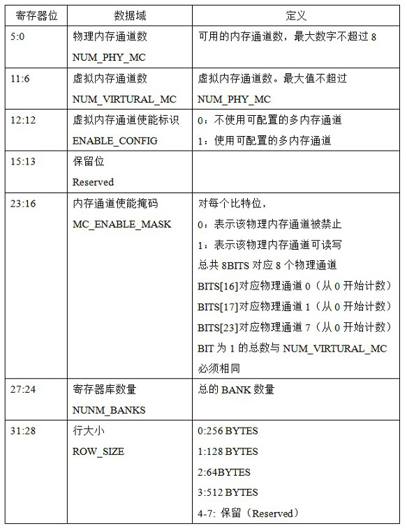
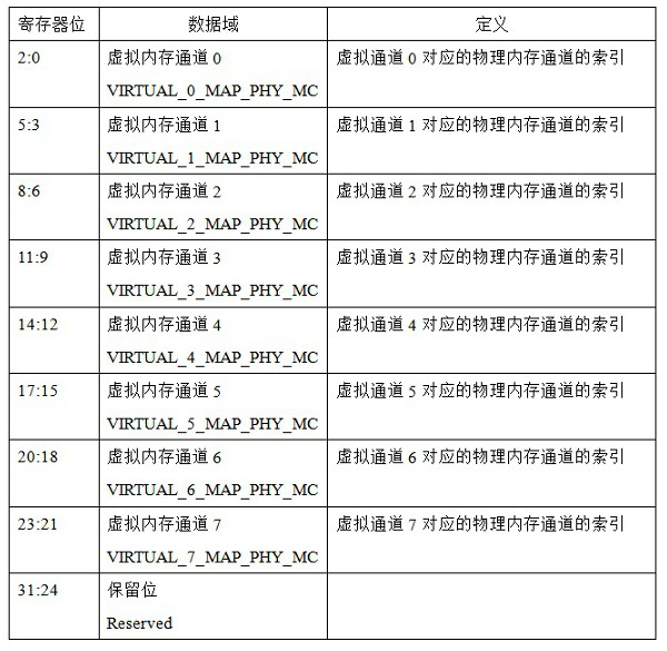
[0064] The technical solutions of the present application will be clearly and completely described below through the embodiments and in conjunction with the accompanying drawings, but the present application is not limited to the embodiments described below. Based on the following embodiments, all other embodiments obtained by persons of ordinary skill in the art without creative efforts fall within the protection scope of the present application. For clarity, parts irrelevant to describing the exemplary embodiments are omitted in the drawings.

[0065] It should be understood that terms such as "comprising" or "having" in this application are intended to indicate the existence of features, numbers, steps, acts, components or combinations thereof disclosed in this specification, and do not exclude one or more other features. , numbers, steps, actions, parts, or combinations thereof exist or are added to. "Multiple" in this application can usually be interpreted as two or more...


PUM


Abstract

The invention discloses a memory access device and method for multiple memory channels and data processing equipment, and relates to the technical field of computer memory access. According to the access device, configuration information of a virtual memory channel and a physical memory channel is set through a configuration register, the configuration information comprises a mapping relation between a virtual memory channel index and a physical memory channel index; the memory management unit calculates and obtains a target virtual memory channel index based on the physical memory address of the memory access request and the configuration information, and calculates and obtains a target physical memory channel index mapped by the target virtual memory channel index based on the target virtual memory channel index and the mapping relation; the storage controller is arranged corresponding to the physical memory channel and controls access to the memory, wherein the storage controller arranged corresponding to the physical memory channel corresponding to the target physical memory channel index performs access to the target data in the target memory according to the physical memory address of the memory access request.

Description

technical field [0001] The present application relates to the technical field of computer memory access, in particular to a multi-memory channel memory access device, method and data processing equipment. Background technique [0002] With the improvement of computing power, the memory channels of chips such as central processing unit (Central Processing Unit, referred to as CPU), graphics processing unit (Graphics Processing Unit, referred to as GPU), artificial intelligence (Artificial Intelligence, referred to as AI) video codec become more and more For example, the first 7nm GPU chip AMD Vega20 contains 32 memory channels. In the future, chips containing more memory channels will be a major trend. [0003] However, the yield rate of chips will drop sharply when the chip is manufactured in a high-tech process below 14 nm. When individual memory channels in the chip are damaged during the manufacturing process, the yield rate will also drop sharply, thereby greatly increa...

Claims


Application Information

Patent Timeline
Patent Type & Authority Applications(China)
IPC IPC(8): G06F9/30G06F15/78
CPCG06F9/30043G06F9/30138G06F9/30141G06F15/7839
Inventor 不公告发明人
Owner METAX INTEGRATED CIRCUITS (SHANGHAI) CO LTD
Learn More