
Device and method for controlling brightness divisions of exposure light sources for liquid crystal panels

A liquid crystal panel, zone control technology, applied in optics, nonlinear optics, instruments, etc., to meet the requirements of equipment takt time, save takt time, and solve the effect of imaging needs

Active Publication Date: 2022-02-22
ZHAOQING ZHONGDAO OPTOELECTRONICS EQUIP CORP
View PDF0 Cites 0 Cited by
  • Summary
  • Abstract
  • Description
  • Claims
  • Application Information

AI Technical Summary

Problems solved by technology

[0009] The purpose of the present invention is to solve the shortcomings of the existing light source control device

Method used


Image

  • Device and method for controlling brightness divisions of exposure light sources for liquid crystal panels
  • Device and method for controlling brightness divisions of exposure light sources for liquid crystal panels
  • Device and method for controlling brightness divisions of exposure light sources for liquid crystal panels

Examples


Embodiment Construction

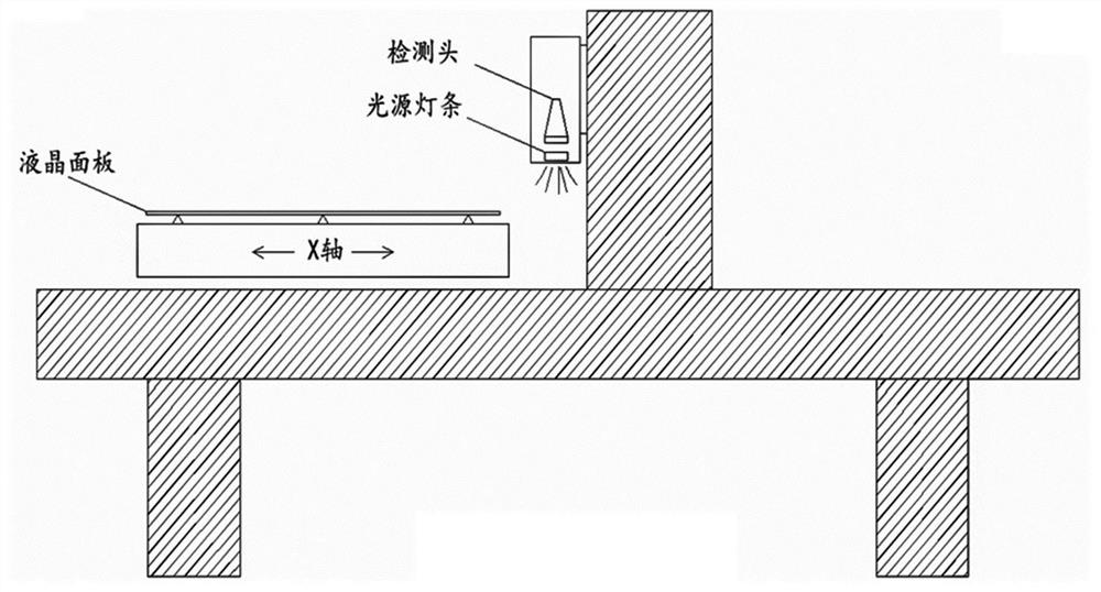
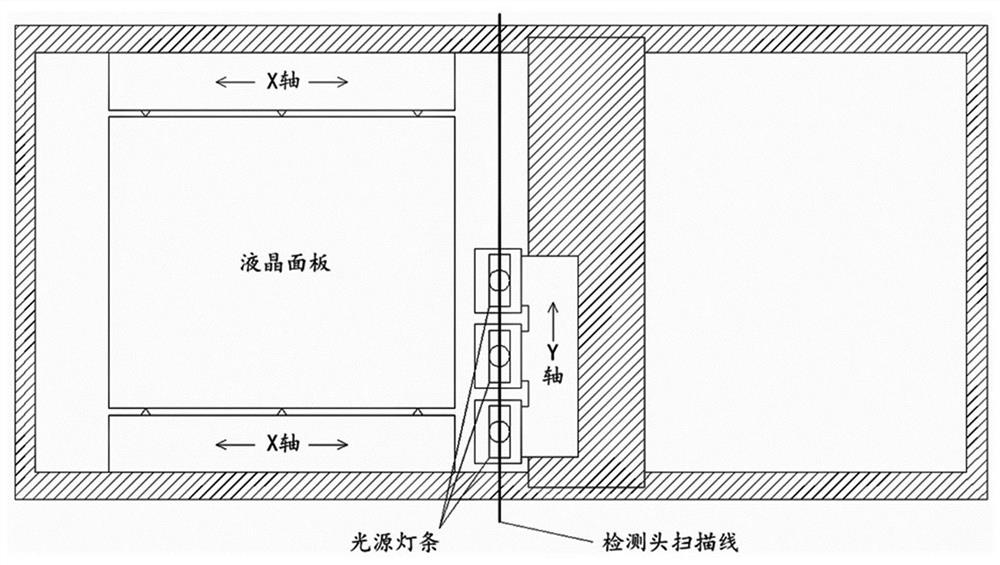
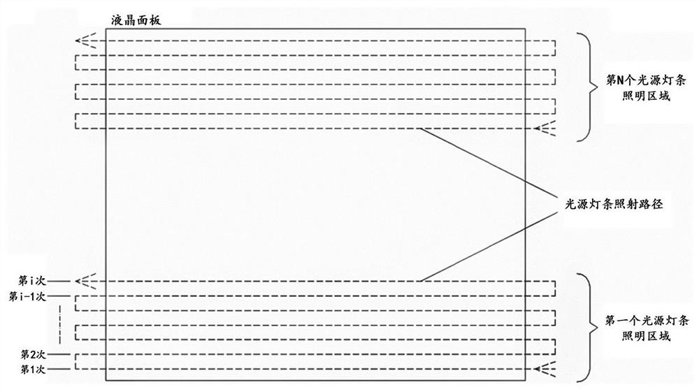
[0049] Exemplary embodiments of the present disclosure will be described in more detail below with reference to the accompanying drawings. Although exemplary embodiments of the present disclosure are shown in the drawings, it should be understood that the present disclosure may be embodied in various forms and should not be limited by the embodiments set forth herein. Rather, these embodiments are provided for more thorough understanding of the present disclosure and to fully convey the scope of the present disclosure to those skilled in the art.

[0050] In the TFT-LCD liquid crystal panel defect detection process, the light reflectance of the array area and the peripheral area of ​​the liquid crystal panel to be inspected is not the same. Under the same brightness, the array area and the peripheral area cannot achieve the best brightness at the same time, and the final imaging cannot reach the optimum. good or even poor, seriously affecting defect detection performance.

[...


PUM


Abstract

The invention discloses a device and a method for controlling brightness divisions of a liquid crystal panel exposure light source. The device includes: a light source light bar controller, at least one lamp bead control unit and an industrial computer connected to the light source light bar controller; , each lamp bead control unit includes a DA conversion circuit and at least one lamp bead arranged in a line, each lamp bead is connected to the output end of the DA conversion circuit, and the input end of the DA conversion circuit is connected to the light source light bar controller I / O ports. The advantages of the present invention are: (1) The array area and the peripheral area can be detected at the same time, and only one defect detection scan is required, which can meet the equipment beat requirement and save the beat time. (2) The light source illumination of small areas can be controlled independently, and the peripheral area and the array area can be sub-area and multi-light intensity illumination. The light source intensity can be controlled independently, and the imaging needs of each area of ​​the liquid crystal panel can be solved.

Description

technical field [0001] The invention belongs to the technical field of liquid crystal panel defect detection, and in particular relates to a device and method for controlling brightness divisions of an exposure light source of a liquid crystal panel. Background technique [0002] The peripheral area of ​​the TFT-LCD liquid crystal panel is the IC&FPC Bonding area, metal wiring and signal pad area. In the past, the industry had no defect detection requirements for the peripheral area. With the development of mobile phone screens and the technological innovation of liquid crystal panels, the peripheral area undertakes more and more important functions, and it has also become an area that must be inspected in defect inspection equipment. However, the roles of the array area and the peripheral area are different, there are differences in materials, processes, and structures, and the reflectivity often varies widely. According to the data, most peripheral areas have strong refle...

Claims


Application Information

Patent Timeline
Patent Type & Authority Patents(China)
IPC IPC(8): G02F1/13
CPCG02F1/1309
Inventor 彭志豪李波
Owner ZHAOQING ZHONGDAO OPTOELECTRONICS EQUIP CORP
Learn More