Quick edge searching method for modular semiconductor surface

A semiconductor and modular technology, applied in image analysis, image enhancement, instruments, etc., can solve problems affecting production capacity, high software requirements, etc., and achieve the effect of increasing speed

Active Publication Date: 2021-12-24
SHANGHAI YINGSHUO ELECTRONICS TECH CO LTD
View PDF4 Cites 0 Cited by
  • Summary
  • Abstract
  • Description
  • Claims
  • Application Information

AI Technical Summary

Problems solved by technology

However, the traditional visual inspection is limited by the frame rate of the camera, the processing power of the industrial computer, and the hardware update, etc. The requirements for the software are very high, and because the update software often needs to modify the main program, which affects the production capacity

Method used


Image

  • Quick edge searching method for modular semiconductor surface
  • Quick edge searching method for modular semiconductor surface

Examples


Embodiment

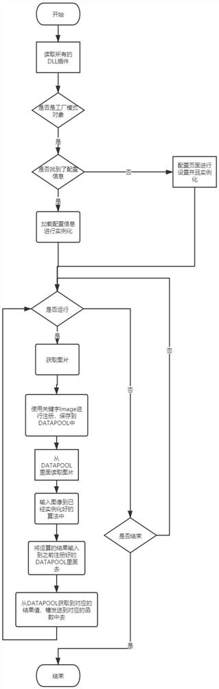
[0057]Embodiment: the algorithm is pre-packaged as a DLL plug-in, and the object of the factory pattern is defined as the plug-in, and the custom factory pattern reads all DLL plug-ins, and judges whether it is an object of the custom factory pattern according to the interface class of the DLL plug-in , if no, end, if yes, the custom factory mode searches for the corresponding configuration information according to the class name of the DLL plug-in, if there is no corresponding configuration information, enter the configuration page to set and instantiate it as an algorithm plug-in, if any, load the corresponding configuration information Instantiate it as an algorithm plug-in, and judge whether the instantiated algorithm plug-in is running. If not, pop up the interface to ask whether it is over. If you choose No, repeat the above operation. If you choose Yes, it will end. If yes, get the input from the configuration information of the storage module And all the mapping informa...


PUM


Abstract

The invention belongs to the technical field of semiconductor integrated circuit device packaging, and particularly relates to a modular semiconductor surface quick edge searching method which comprises the following steps: firstly, reading class names of all DLL plug-ins, judging whether the DLL plug-ins are objects of a factory mode according to interface classes, secondly, searching corresponding configuration information according to the class names, If yes, executing the step 3; loading corresponding configuration information for instantiation, if not, setting the corresponding configuration information and performing instantiation, then judging whether the instantiated DLL plug-in runs or not, if not, ending inquiry or not, if yes, collecting a picture, registering by using a keyword and storing the picture into a data pool, then starting an algorithm plug-in, extracting the picture from the data pool for edge searching, If not, executing the step of searching the edge of the picture. And inputting an operation result into a registered data pool, and finally, collecting a corresponding result value from the data pool, and transmitting the result value to a corresponding module through a slot signal for subsequent image operation. Based on the method, the influence of software updating on the productivity can be reduced, and the semiconductor surface defect detection speed is increased.

Description

technical field [0001] The invention belongs to the technical field of packaging of semiconductor integrated circuit devices, and in particular relates to a fast edge-finding method for a modularized semiconductor surface. Background technique [0002] In the semiconductor industry, high-speed production activities are often required, so when performing on-line detection of surface defects on semiconductors, a certain speed is also required to ensure production efficiency. However, the traditional visual inspection is limited by the frame rate of the camera, the processing power of the industrial computer, and the hardware update. It has high requirements for the software, and because the update of the software often requires the modification of the main program, which affects the production capacity. [0003] Therefore, it is necessary to design a fast edge-finding method for modularized semiconductor surfaces, which can reduce the impact of software updates on production c...

Claims


Application Information

Patent Timeline
Patent Type & Authority Applications(China)
IPC IPC(8): G06T7/13G06T7/11G06T7/70
CPCG06T7/13G06T7/11G06T7/70G06T2207/30148
Inventor 袁林彦伊沃章伟
Owner SHANGHAI YINGSHUO ELECTRONICS TECH CO LTD
Why Eureka
Try Eureka