Cutting device for semiconductor

A cutting device, semiconductor technology, applied in the direction of cutting device, cutting machine, metal processing equipment, etc., can solve the problems of semiconductor limit, easy clamping instability, device does not have adaptability, etc., to achieve the effect of ensuring cleanliness

Pending Publication Date: 2022-01-14
张浩
View PDF7 Cites 0 Cited by
  • Summary
  • Abstract
  • Description
  • Claims
  • Application Information

AI Technical Summary

Problems solved by technology

[0003] At present, the semiconductor cutting device is very mature, but it is difficult to limit the position of the semiconductor during the cutting process. A clamping device is needed for clamping, and the general semiconductor clamping cannot achieve the expected effect, and it is easy to clamp incorrectly. Stable or offset, when fixing cylindrical semiconductor materials, it often needs to be fixed in the horizontal or vertical direction, and the existing devices do not have good adaptability

Method used


Image

  • Cutting device for semiconductor
  • Cutting device for semiconductor
  • Cutting device for semiconductor

Examples


Embodiment Construction

[0030] The following will clearly and completely describe the technical solutions in the embodiments of the present invention with reference to the accompanying drawings in the embodiments of the present invention. Obviously, the described embodiments are only some, not all, embodiments of the present invention.

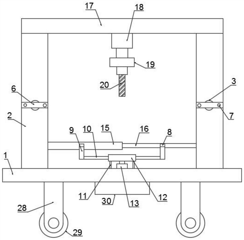
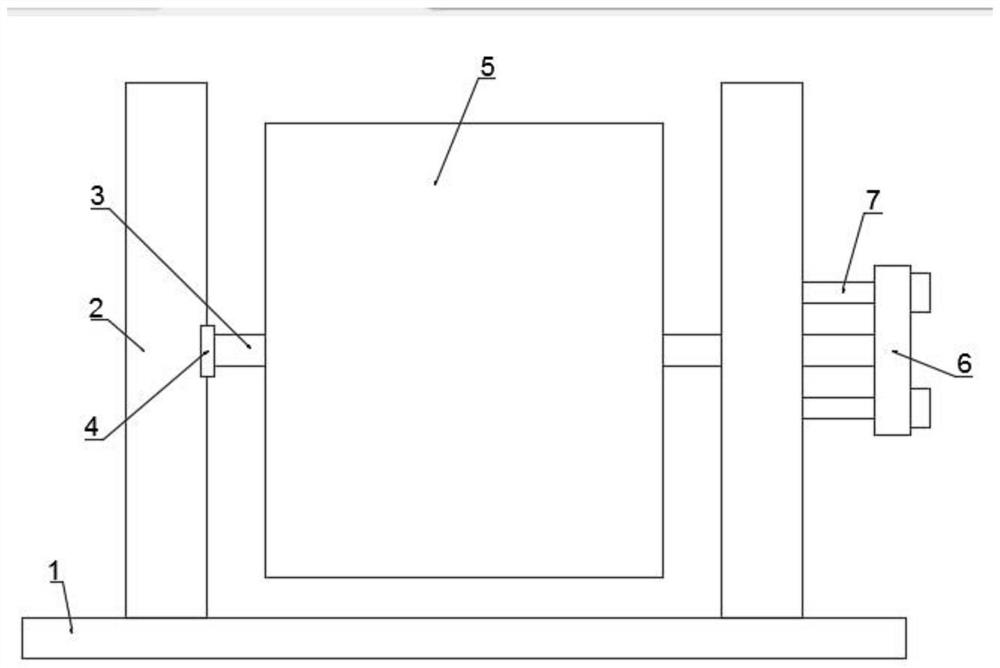
[0031] refer to Figure 1-7 , a cutting device for semiconductors, comprising a base 1, the upper side wall of the base 1 is symmetrically slidably connected with a vertical plate 2, the upper side wall of the base 1 is symmetrically provided with a chute matching the vertical plate 2, and the A rotating shaft 3 extending to the front side is rotatably connected between the two vertical plates 2, and a bearing 4 is fixedly embedded in the front side wall of the vertical plate 2 on the rear side of the same side, and the inner ring of each bearing 4 is connected to the rotating shaft. The outer walls of 3 are fixedly connected, and the front ends of the rotating shaft...


PUM


Abstract

The invention discloses a cutting device for a semiconductor. The cutting device comprises a base, wherein vertical plates are symmetrically and slidably connected to the upper side wall of the base, rotating shafts extending to the front side are rotationally connected between the two vertical plates located on the same side, rotating plates are fixedly connected to the front ends of the rotating shafts located on the same side, and bolts which are in contact with the outer walls of the vertical plates in an abutting mode are symmetrically connected to the outer walls of the rotating plates located on the same side in a threaded mode. According to the cutting device, clamping plates move in the direction close to the outer wall of a semiconductor material, so that the clamping plates are tightly attached to the semiconductor material, then the semiconductor material is rapidly fixed, and therefore the stability of the semiconductor during cutting is guaranteed; arc-shaped grooves and cylindrical grooves are formed in the clamping plates, so that the semiconductor material can be fixedly clamped in the vertical direction or the horizontal direction; the cutting device can well adapt to the cutting position through the change of the clamping direction; and a sweeping mechanism is arranged, so that the cleanliness of the device during use is guaranteed.

Description

technical field [0001] The invention relates to the technical field of semiconductors, in particular to a cutting device for semiconductors. Background technique [0002] A semiconductor refers to a material whose conductivity at room temperature is between that of a conductor and an insulator. Semiconductors are used in integrated circuits, consumer electronics, communication systems, photovoltaic power generation, lighting applications, high-power power conversion and other fields. For example, a diode is a device made of a semiconductor. No matter from the perspective of technology or economic development, the importance of semiconductors is enormous. The core units of most of today's electronic products, such as computers, mobile phones or digital recorders, are closely related to semiconductors. Common semiconductor materials include silicon, germanium, gallium arsenide, etc., and silicon is the most influential one in commercial applications among various semiconduc...

Claims


Application Information

Patent Timeline
Patent Type & Authority Applications(China)
IPC IPC(8): B23G1/44
CPCB23G1/44
Inventor 张浩
Owner 张浩
Why Eureka
Try Eureka