Supercharge Your Innovation With Domain-Expert AI Agents!

Semiconductor epitaxial structure and preparation method thereof

An epitaxial structure, semiconductor technology, applied in semiconductor/solid state device manufacturing, semiconductor devices, chemical instruments and methods, etc., can solve the problems of high cost, low epitaxial growth efficiency, etc., to improve adhesion, reduce particle drop and even The effect of the probability of falling off

Active Publication Date: 2022-01-14
SUZHOU EVERBRIGHT PHOTONICS CO LTD +1
View PDF8 Cites 0 Cited by
  • Summary
  • Abstract
  • Description
  • Claims
  • Application Information

AI Technical Summary

Problems solved by technology

[0004] Therefore, the technical problem to be solved by the present invention is to overcome the problems of low epitaxial growth efficiency and high cost in the prior art, thereby providing a semiconductor epitaxial structure and its preparation method

Method used


Image

  • Semiconductor epitaxial structure and preparation method thereof
  • Semiconductor epitaxial structure and preparation method thereof
  • Semiconductor epitaxial structure and preparation method thereof

Examples


preparation example Construction

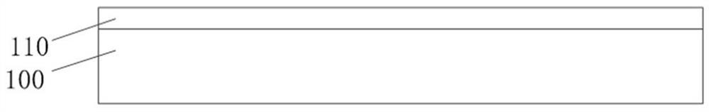
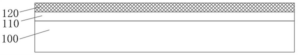
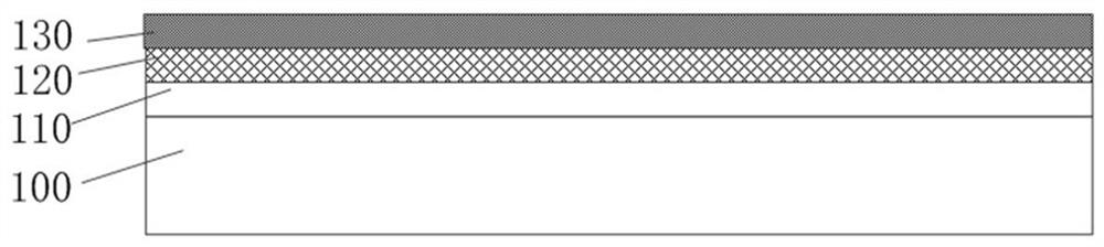
[0034] On this basis, an embodiment of the present invention provides a method for preparing a semiconductor epitaxial structure, including: forming a first semiconductor epitaxial structure on the surface of an accessory in a chamber of an epitaxial growth device; the method for forming the first semiconductor epitaxial structure includes : form an adhesion semiconductor layer on the surface of the accessory; form a gettering transition semiconductor layer on the surface of the adhesion semiconductor layer facing away from the accessory; form a gettering transition semiconductor layer on the surface of the gettering transition semiconductor layer One side of the semiconductor layer forms a first base semiconductor material layer; the adhesion between the material of the adhesive semiconductor layer and the fitting is greater than the adhesion between the material of the gettering transition semiconductor layer and the fitting sex.

[0035]Due to the formation of the adhesive ...


PUM


Abstract

The invention provides a semiconductor epitaxial structure and a preparation method thereof. The preparation method of the semiconductor epitaxial structure comprises the steps of forming a semiconductor epitaxial structure on the surface of an accessory in a cavity of epitaxial growth equipment, wherein the method for forming the semiconductor epitaxial structure comprises the steps of forming an adhesive semiconductor layer on the surface of the accessory; forming a gettering transition semiconductor layer on the surface of the side, which is opposite to the accessory, of the adhesive semiconductor layer; and forming a first base layer semiconductor material layer on the side, which is back to the adhesive semiconductor layer, of the gettering transition semiconductor layer. The adhesion between the material of the adhesive semiconductor layer and the accessory is greater than the adhesion between the material of the gettering transition semiconductor layer and the accessory. The preparation method of the semiconductor epitaxial structure enables epitaxial growth to be high in efficiency and low in cost.

Description

technical field [0001] The invention relates to the technical field of semiconductors, in particular to a semiconductor epitaxial structure and a preparation method thereof. Background technique [0002] Metal-organic vapor deposition (MOCVD) technology is a commonly used production method for III-V semiconductor materials at the present stage, but the particles falling off the surface of graphite and quartz parts in the reaction chamber of MOCVD machines and the epitaxial defects caused by them have always troubled semiconductor materials. A difficult problem in epitaxial growth, which is mainly due to the drop of particles in the reaction chamber and the resulting epitaxial defects will cause a series of reliability problems such as power drop, functional failure, and shortened life of III-V semiconductor materials in subsequent use. . When III-V semiconductor materials are used in miniaturized, integrated, and energy-efficient devices or scenarios, more stringent require...

Claims


Application Information

Patent Timeline
IPC IPC(8): H01L21/02H01L29/205C30B29/68C30B29/40C30B29/42C30B25/02
CPCH01L21/02538H01L21/02546H01L21/0262H01L21/02455H01L21/02463H01L21/02461H01L29/205C30B29/68C30B29/40C30B29/42C30B25/02
Inventor 郭银涛程洋肖啸王俊胡耀东夏明月方砚涵
Owner SUZHOU EVERBRIGHT PHOTONICS CO LTD
Features
  • R&D
  • Intellectual Property
  • Life Sciences
  • Materials
  • Tech Scout
  • Unparalleled Data Quality
  • Higher Quality Content
  • 60% Fewer Hallucinations
Learn More