Semiconductor structure and forming method thereof

A semiconductor and wet etching technology, used in semiconductor devices, semiconductor/solid-state device manufacturing, transistors, etc., can solve the problems of difficult channel, poor gate-to-channel control ability, etc., and improve fin bending. , performance improvement, the effect of reducing the extrusion force

Pending Publication Date: 2022-01-25
SEMICON MFG INT (SHANGHAI) CORP +1
View PDF0 Cites 0 Cited by
  • Summary
  • Abstract
  • Description
  • Claims
  • Application Information

AI Technical Summary

Problems solved by technology

However, as the channel length of the device is shortened, the distance between the source and the drain of the device is also shortened, so the control ability of the gate to the channel becomes worse, and the gate vol

Method used


Image

  • Semiconductor structure and forming method thereof
  • Semiconductor structure and forming method thereof
  • Semiconductor structure and forming method thereof

Examples


Embodiment Construction

[0012] The performance of current semiconductor structures needs to be improved. Combining with a method of forming a semiconductor structure, the reason why its performance needs to be improved is analyzed.

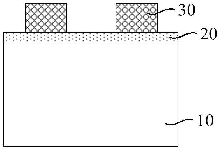
[0013] Figure 1 to Figure 4 It is a structural schematic diagram corresponding to each step in a method for forming a semiconductor structure.

[0014] refer to figure 1 , providing a substrate 10 , forming a buffer layer 20 and a mask layer 30 on the buffer layer 20 on the substrate 10 .

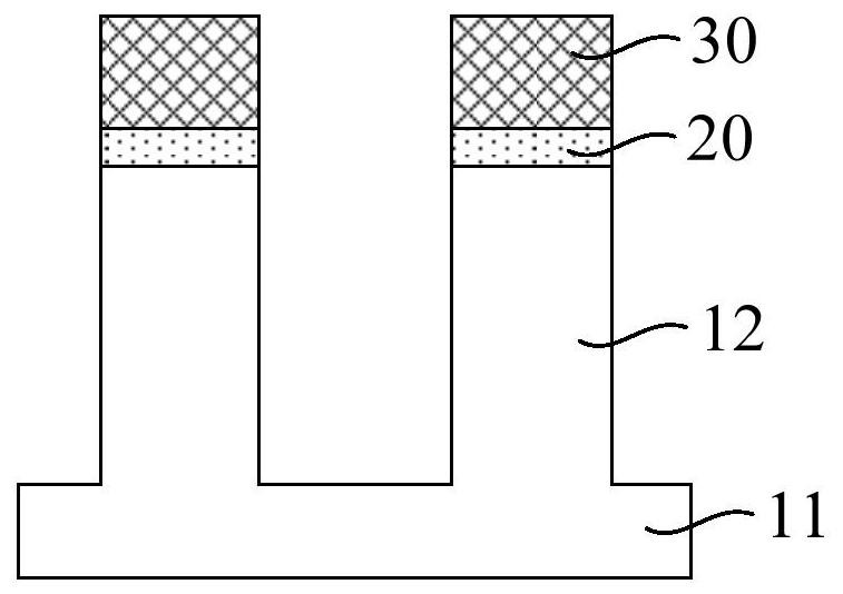
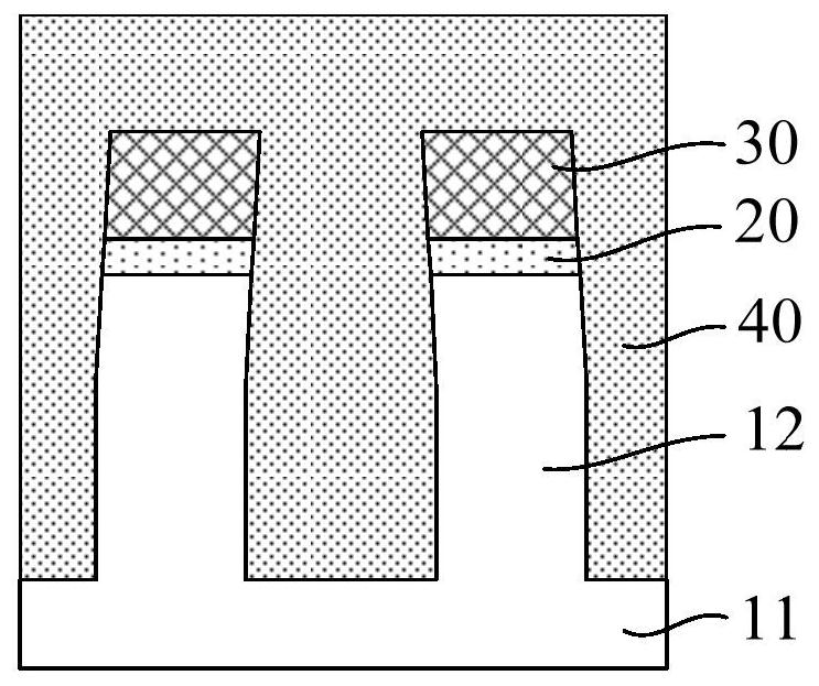
[0015] refer to figure 2 , using the mask layer 30 as a mask, sequentially etching the buffer layer 20 and the base 10 to form the substrate 11 and the fins 12 protruding from the substrate 11 .

[0016] refer to image 3 , forming an isolation material layer 40 on the substrate 11 , the isolation material layer 40 fills between the fins 12 and covers the top of the mask layer 30 .

[0017] refer to Figure 4 , using the top of the mask layer 30 as a stop position, planarize ...


PUM


Abstract

The invention discloses a semiconductor structure and a forming method thereof. The forming method comprises the steps of providing a substrate; forming a mask layer on the substrate; forming a compensation side wall on the side wall of the mask layer; etching the base by taking the mask layer and the compensation side wall as masks to form a substrate and fin parts protruding out of the substrate; removing the compensation side wall; and after the compensation side wall is removed, forming an isolation layer covering part of the side wall of the fin part on the substrate exposed out of the fin part. After the fin parts are formed, the compensation side walls are removed, then the isolation layer is formed, the process of forming the isolation layer comprises the step of filling the space between the fin parts with the isolation material layer, the size of the top opening of the opening defined by the mask layer, the fin parts and the substrate is large by removing the compensation side walls, and therefore in the process of depositing the isolation material layer, the bottom of the opening is easily filled with the isolation material layer, so the probability of accumulation of the isolation material layer at the top of the fin part is reduced, the extrusion force of the isolation material layer on the fin part is reduced, the problem of fin part bending is improved, and the performance of the semiconductor structure is improved.

Description

technical field [0001] Embodiments of the present invention relate to the field of semiconductor manufacturing, and in particular, to a semiconductor structure and a method for forming the same. Background technique [0002] In semiconductor manufacturing, with the development trend of VLSI, the feature size of integrated circuits continues to decrease. In order to accommodate the reduction in feature size, the channel length of MOSFETs has also been shortened accordingly. However, as the channel length of the device is shortened, the distance between the source and the drain of the device is also shortened, so the control ability of the gate to the channel becomes worse, and the gate voltage pinches off the channel. Difficulty is also increasing, making the phenomenon of subthreshold leakage (subthreshold leakage), the so-called short-channel effects (short-channel effects, SCE) more likely to occur. [0003] Therefore, in order to better adapt to the reduction of the fea...

Claims


Application Information

Patent Timeline
IPC IPC(8): H01L21/8234H01L27/088
CPCH01L21/823431H01L21/823468H01L27/0886
Inventor 郑二虎张海洋
Owner SEMICON MFG INT (SHANGHAI) CORP
Why Eureka
Try Eureka