Ultraviolet-near infrared broadband photoconductive detector

An ultraviolet band and near-infrared technology, applied in semiconductor devices, electrical components, circuits, etc., can solve the problems of low optical responsivity, narrow band range, and difficulty in realizing dual-band detection, and achieve the effect of broadening the spectral response range.

Inactive Publication Date: 2022-02-01
TIANJIN JINHANG INST OF TECH PHYSICS
View PDF0 Cites 0 Cited by
  • Summary
  • Abstract
  • Description
  • Claims
  • Application Information

AI Technical Summary

Problems solved by technology

In the visible and near-infrared, photodetectors are mainly used in ray measurement and detection, industrial automatic control, photometric measurement, etc.; photodetectors based on silicon and GaAs are increasingly mature in the visible and near-infrared. It is difficult for material systems to reali

Method used


Image

  • Ultraviolet-near infrared broadband photoconductive detector
  • Ultraviolet-near infrared broadband photoconductive detector
  • Ultraviolet-near infrared broadband photoconductive detector

Examples


Embodiment 1

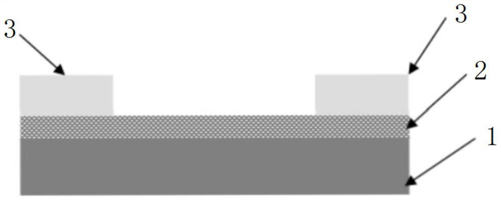
[0024] Please refer to figure 1 The shown structural schematic diagram of the first embodiment of a UV-near-infrared broadband photoconductive detector provided by the present application includes:

[0025] The GaAs material substrate layer 1 has good light absorption characteristics and high responsivity in the near-infrared band, and can be used to detect the near-infrared wide band; here, the type of the GaAs material substrate layer 1 is, for example, n- or p-light doped substrate structure, and its thickness is 0.3-0.5 mm;

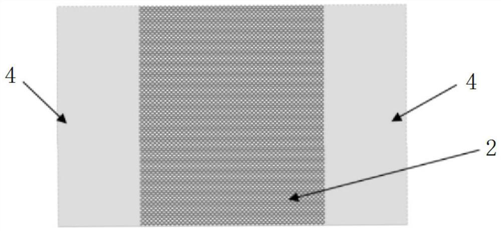
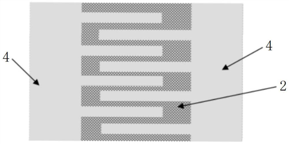
[0026] Bi 2 Se 3 The material layer 2 is arranged on the upper surface of the GaAs material substrate layer 1. It has good light absorption characteristics in the ultraviolet and visible light bands, and is easy to integrate with other semiconductor materials, and can be used to detect the ultraviolet band; here, Bi 2 Se 3 The thickness of material layer 2 is 20-100nm;

[0027] Among them, Bi 2 Se 3 The material layer 2 can be directly grown on...


PUM

PropertyMeasurementUnit
Thicknessaaaaaaaaaa
Thicknessaaaaaaaaaa

Abstract

The invention discloses an ultraviolet-near infrared broadband photoconductive detector. The ultraviolet-near infrared broadband photoconductive detector comprises a GaAs material substrate layer, a Bi2Se3 material layer arranged on the upper surface of the GaAs material substrate layer, and an electrode layer arranged on the upper surface of the Bi2Se3 material layer. By adjusting the voltage applied to the electrode layer, the GaAs material substrate layer can detect a near-infrared broadband, and the Bi2Se3 material layer can detect an ultraviolet waveband. The GaAs material substrate layer and the Bi2Se3 material layer are specifically designed, the Bi2Se3 material layer is arranged on the upper surface of the GaAs material substrate layer, the GaAs material substrate layer and the Bi2Se3 material layer can form a longitudinally vertical heterojunction structure, and the spectral response range is effectively widened; and the electrode layer is arranged on the upper surface of the Bi2Se3 material layer, the GaAs material substrate layer can detect the near-infrared broadband, the Bi2Se3 material layer can detect the ultraviolet waveband by adjusting the voltage applied to the electrode layer, and ultraviolet-near-infrared broadband detection is achieved.

Description

technical field [0001] The present disclosure generally relates to the technical field of semiconductor photodetectors, in particular to an ultraviolet-near-infrared broadband photoconductive detector. Background technique [0002] Photodetectors are widely used in various fields such as national economy and military affairs. Photodetectors based on detection in different wavelength bands play an important role in the detection of different fields. In the visible and near-infrared, photodetectors are mainly used in ray measurement and detection, industrial automatic control, photometric measurement, etc.; photodetectors based on silicon and GaAs are increasingly mature in the visible and near-infrared. It is difficult for material systems to achieve dual-band detection of ultraviolet and near-infrared. Therefore, we propose an ultraviolet-near-infrared broadband photoconductive detector to solve the above-mentioned problems of low photoresponsivity, narrow wavelength range...

Claims


Application Information

Patent Timeline
IPC IPC(8): H01L31/0304H01L31/032H01L31/101H01L31/109
CPCH01L31/1013H01L31/109H01L31/0304H01L31/032
Inventor 张云霄李爱民孙文宝
Owner TIANJIN JINHANG INST OF TECH PHYSICS
Why Eureka
Try Eureka