Automatic antenna chip welding device for RFID (Radio Frequency Identification Device) production

An automatic welding and chip technology, applied in the field of RFID, can solve problems such as hindering the welding work of devices, reducing the yield of finished products, and reducing welding efficiency, so as to reduce production costs, prevent false welding, and improve production efficiency.

Active Publication Date: 2022-02-18
深圳市美师傅科技有限公司
View PDF7 Cites 0 Cited by
  • Summary
  • Abstract
  • Description
  • Claims
  • Application Information

AI Technical Summary

Problems solved by technology

[0002] When welding the RFID antenna and the chip, the existing technology is prone to false welding, which leads to the weak welding of the antenna and the chip, and there are also cases where the antenna and the chip are welded badly , reduce the yield of finished products;
[0003]Secondly, the solder itself is relatively soft, and it is prone to bending during welding. It needs to be straightened manually, which reduces the welding efficiency, affects the welding effect, and hinders the device Perform welding work, or even cause direct damage to the welding device

Method used


Image

  • Automatic antenna chip welding device for RFID (Radio Frequency Identification Device) production
  • Automatic antenna chip welding device for RFID (Radio Frequency Identification Device) production
  • Automatic antenna chip welding device for RFID (Radio Frequency Identification Device) production

Examples


Embodiment 1

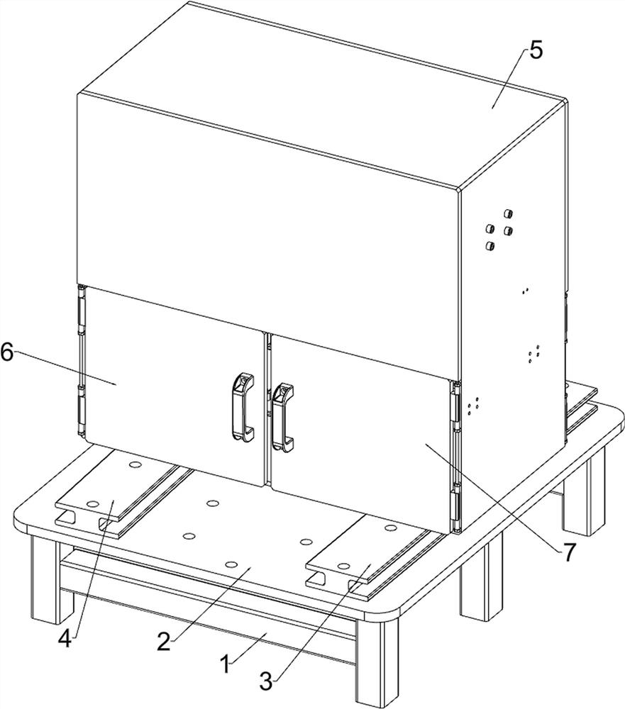
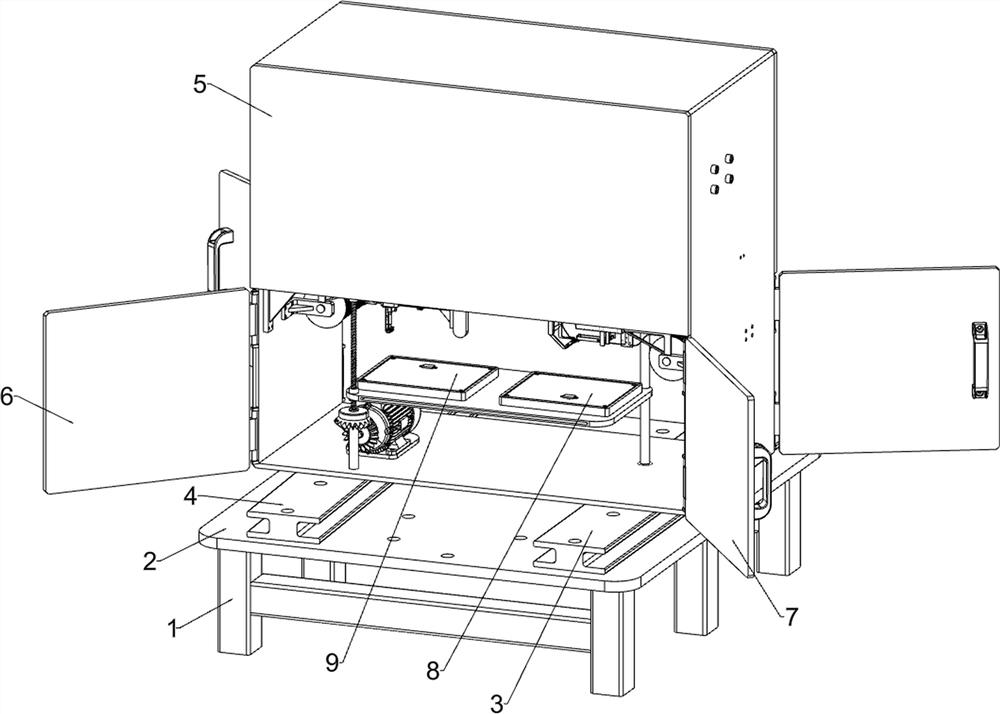
[0038] An automatic welding device for RFID production antenna chips, such as Figure 1-13 As shown, it includes a fixing frame 1, a bottom plate 2, a first bolt fixing plate 3, a second bolt fixing plate 4, a protective frame 5, a first hatch 6, a second hatch 7, a first analog chip 8, a second Analog chip 9, welding assembly, chip conveying assembly, solder conveying assembly and antenna conveying assembly; the upper side of the fixing frame 1 is fixedly connected with the bottom plate 2; The left part is fixedly connected with a second bolt fixing plate 4; the upper side of the first bolt fixing plate 3 and the upper side of the second bolt fixing plate 4 are equipped with a protective frame 5; the lower side of the protective frame 5 is equipped with a first hatch 6; A second hatch 7 is installed below the front side of the frame 5, and the second hatch 7 is positioned at the right side of the first hatch 6; group; the inner upper part of the protective frame 5 is bolt-co...

Embodiment 2

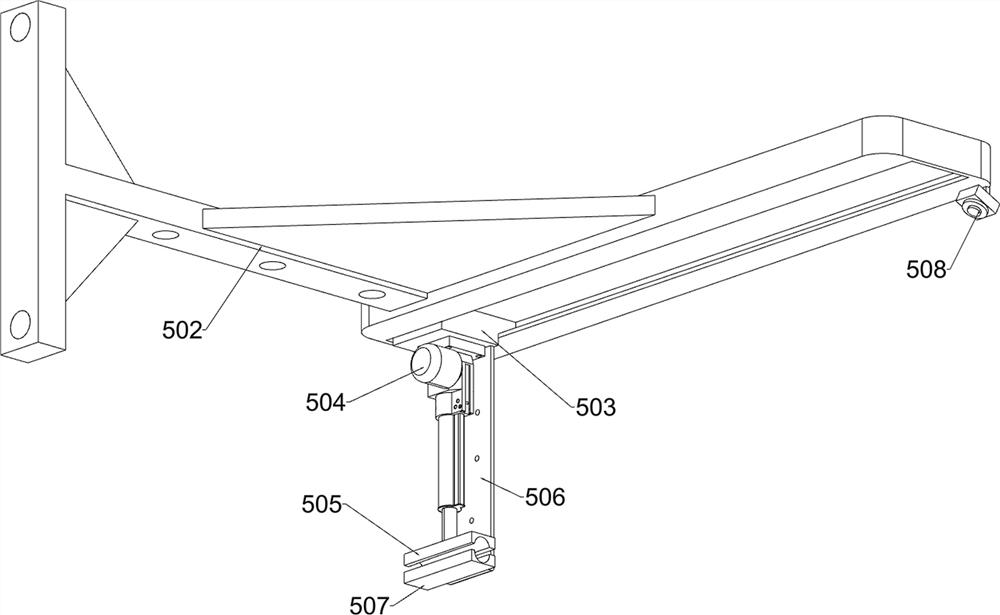
[0047] On the basis of Example 1, such as figure 1 , figure 2 , image 3 , Figure 14 with Figure 15 As shown, it also includes a solder overflow prevention assembly, which is located on the lower side of the solder delivery assembly, and the solder overflow prevention assembly includes a first connecting frame 601, a second connecting frame 602 and a limit frame 603; the fifth driving part 408 The first connecting frame 601 is fixedly connected to the lower side; the second connecting frame 602 is fixedly connected to the lower side of the sixth driving part 409; One connecting frame 601 and the second connecting frame 602 are all provided with one on the lower side of the two fifth driving parts 408 and the sixth driving part 409; A spacer 603 is connected.

[0048] When the 8-first analog chip and the 9-second analog chip rise to the above-mentioned height, one side of the 8-first analog chip and the 9-second analog chip are respectively in contact with the protrudin...

Embodiment 3

[0050] On the basis of Example 2, such as figure 1 , figure 2 , image 3 , Figure 16 , Figure 17 with Figure 18 As shown, a solder processing assembly is also included, the solder processing assembly is located on the upper side of the welding assembly, and the solder processing assembly includes a seventh connecting plate 701, an eleventh driving component 702, an eighth connecting plate 703, and a fifth L-shaped connecting plate 704 , the first telescopic part 705, the second telescopic part 706, the third telescopic part 707, the ninth connecting plate 708, the push plate 709, the limit protection block 7010 and the push block 7011; The connecting plate 701; the eleventh drive part 702 is fixedly connected to the lower side of the seventh connecting plate 701; the eighth connecting plate 703 is fixedly connected to the lower side of the eleventh driving part 702; the fifth connecting plate 703 is fixedly connected to the lower side L-shaped connecting plate 704; th...


PUM


Abstract

The invention relates to the field of RFID, in particular to an automatic antenna chip welding device for RFID production. The invention aims to solve the technical problems that pseudo soldering and welding damage exist between an antenna and a chip, soldering tin is bent, the welding efficiency is influenced, and even the antenna and the chip are damaged. According to the technical scheme, the automatic antenna chip welding device for RFID production comprises a bottom plate, a first bolt fixing plate, a second bolt fixing plate and the like; the right part of the upper surface of the bottom plate is in bolted connection with a first bolt fixing plate; and the second bolt fixing plate is fixedly connected to the left of the upper surface of the bottom plate. According to the invention, while the automatic welding of the RFID chip and the antenna is realized, the welding point of the RFID chip is welded with a layer of bottom tin in advance, so that the condition of pseudo soldering between the RFID chip and the antenna is effectively prevented, and secondly, the welding tin can be prevented from overflowing to other parts of the RFID chip in the welding process to damage the RFID chip and seriously and directly cause the scrapping of the RFID chip, the production cost is effectively reduced and the production benefit is improved.

Description

technical field [0001] The invention relates to the field of RFID, in particular to an automatic welding device for antenna chips used in RFID production. Background technique [0002] When welding the RFID antenna and chip, the existing technology is prone to false welding, resulting in weak welding of the antenna and chip, and there are also cases where the antenna and chip are welded badly, reducing the yield of finished products; [0003] Secondly, the solder itself is relatively soft, and it is prone to bending during welding. It needs to be straightened manually, which reduces the welding efficiency, affects the welding effect, hinders the welding work of the device, and even causes direct damage to the welding device. Contents of the invention [0004] In order to overcome the shortcoming of false welding and welding damage between the antenna and the chip during welding, the solder will bend, affect the welding efficiency, and even damage the antenna and the chip. ...

Claims


Application Information

Patent Timeline
IPC IPC(8): B23K1/00B23K3/04B23K3/06B23K3/08
CPCB23K3/08B23K1/0016B23K3/0607B23K3/04B23K3/087
Inventor 钱芳
Owner 深圳市美师傅科技有限公司
Why Eureka
Try Eureka