Semiconductor structure and forming method thereof

A technology of semiconductor and metal interconnection structure, applied in the direction of semiconductor device, semiconductor/solid-state device manufacturing, semiconductor/solid-state device components, etc., can solve the problems affecting the electrical performance of the device and so on

Pending Publication Date: 2022-03-01
CHANGXIN MEMORY TECH INC
View PDF0 Cites 0 Cited by
  • Summary
  • Abstract
  • Description
  • Claims
  • Application Information

AI Technical Summary

Problems solved by technology

[0003] With the continuous shrinking of the process line width, the increase of the resistance between the metal layers will become more and more s

Method used


Image

  • Semiconductor structure and forming method thereof
  • Semiconductor structure and forming method thereof
  • Semiconductor structure and forming method thereof

Examples


Embodiment Construction

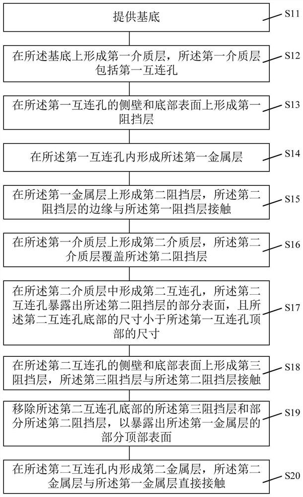
[0053] The specific implementation manners of the present application will be described in detail below in conjunction with the accompanying drawings. When describing the embodiments of the present application in detail, for the convenience of explanation, the schematic diagrams will not be partially enlarged according to the general scale, and the schematic diagrams are only examples, which should not limit the protection scope of the present application. In addition, the three-dimensional space dimensions of length, width and depth should be included in actual production.

[0054] refer to figure 1 , some embodiments of the present application provide a method for forming a semiconductor structure, including the steps of:

[0055] Step S11, providing a substrate;

[0056] Step S12, forming a first dielectric layer on the substrate, the first dielectric layer including first interconnection holes;

[0057] Step S13, forming a first barrier layer on the sidewall and bottom ...


PUM


Abstract

The invention discloses a semiconductor structure and a forming method thereof. The semiconductor structure comprises a substrate; the first dielectric layer is located on the substrate, and the first dielectric layer comprises a first interconnection hole; the first barrier layer covers the inner wall and the bottom of the first interconnection hole; the first metal layer is located in the first interconnection hole; a second barrier layer covering an edge region of a top surface of the first metal layer; the second dielectric layer is located on the first dielectric layer, the second dielectric layer comprises a second interconnection hole, the second interconnection hole exposes a part of the top surface of the first metal layer, and the size of the bottom of the second interconnection hole is smaller than that of the top of the first interconnection hole; the third barrier layer covers the side wall of the second interconnection hole, and the third barrier layer is in contact with the second barrier layer; and the second metal layer is located in the second interconnection hole, and the second metal layer is in direct contact with the first metal layer. The contact resistance between the metal layers of the semiconductor structure is reduced.

Description

technical field [0001] The present application relates to the field of semiconductors, in particular to a semiconductor structure and a method for forming the same. Background technique [0002] The manufacture of semiconductor integrated circuits is an extremely complicated process, aiming to shrink and manufacture various electronic components and circuits of a specific circuit on a semiconductor substrate. After the feature size (CD) of semiconductor devices enters the deep submicron stage, in order to obtain faster computing speed, larger data storage capacity and more functions, this requires that the integration level of semiconductor devices needs to be continuously improved. The number and density of layers increases accordingly. [0003] As the line width of the manufacturing process continues to shrink, the resistance between the metal layers will increase more significantly, which will bring about the problem of RC delay (delay) of the metal interconnection and a...

Claims


Application Information

Patent Timeline
IPC IPC(8): H01L23/538H01L21/768
CPCH01L23/5386H01L21/76895
Inventor 刘洋
Owner CHANGXIN MEMORY TECH INC
Why Eureka
Try Eureka