[0030] Below in conjunction with accompanying drawing, the present invention is further explained and illustrated.
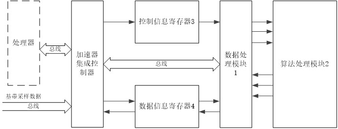
[0031] like figure 1 As shown, an anti-interference channel demodulation accelerator suitable for satellite baseband processing chips includes a data processing module 1, an algorithm processing module 2, a control information register 3 and a data information register 4;
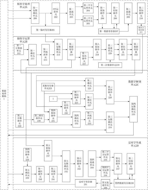
[0032] The data processing module 1 is used to analyze the multi-user control parameters sent by the control information register 3 under the control of the accelerator integrated controller, complete parameter processing, channel identification and data formatting operations, generate local data, and analyze the data information The multi-user data information sent by the register 4 is accessed, and the user data extracted on demand, locally generated data and formatted control information are output to the algorithm processing module 2; The demodulation results and timing word results are buffered and output under the control of the accelerator integrated controller;
[0033] The algorithm processing module 2 is used to perform anti-interference demodulation algorithm processing on the user data, locally generated data and formatted control information sent by the data processing module 1, and obtain the data word demodulation result and the timing word result after processing, and process the The result is output to the data processing module 1;
[0034] The control information register 3 includes a plurality of register groups, which are used to store the multi-user control parameters input by the accelerator integrated controller or processor according to a certain format for reading by the data processing module 1;
[0035] The data information register 4 is used to buffer the baseband sampling data sent from the outside under the control of the accelerator integrated controller, and divide the baseband sampling data into multiple channels according to the multi-user data access rules and output them to the data processing module 1 .
[0036] like figure 2 As shown, the algorithm processing module 2 includes a frequency word processing unit 2A, a unique word operation unit 2B, a data word demodulation unit 2C and a timing word generation unit 2D;
[0037] The frequency word processing unit 2A is used to receive the extracted user data and locally generated data output by the data processing module 1, process and generate demodulated data and frequency word values, and output the demodulated data to the unique word operation unit 2B, and the frequency word values are respectively Output to the unique word operation unit 2B and the data word demodulation unit 2C; the unique word operation unit 2B receives the demodulated data and the frequency word value input by the frequency word processing unit 2A for processing, and produces the unique word and the channel word result of removing the frequency offset, Wherein the unique word result of removing the frequency offset is output to the timing word generation unit 2D, and the channel word result is output to the data word demodulation unit 2C; the data word demodulation unit 2C is used for frequency word value, channel word result and data processing module 1 output The extracted user data is processed to obtain the data word demodulation result, which is output back to the corresponding access unit of the data processing module 1; the timing word generation unit 2D is used to control the unique word result of frequency offset removal and the output of the data processing module 1 The information is processed to obtain the timing word result, which is output back to the corresponding access unit of the data processing module 1.
[0038] Wherein, the frequency word processing unit 2A includes a first complex multiplication unit 200, a first temporary register 201, a first FFT operation unit 202, a first gating unit 203, a first square operation unit 204, and a second square operation unit 205, the first accumulator unit 206, the first data register 207, the first comparator unit 208, the second gating unit 209, the second accumulator unit 210 and the frequency word register 211;
[0039] The first complex multiplication unit 200 performs a complex multiplication operation on the extracted user data output by the data processing module 1 and locally generated data, and the product results are respectively output to the first temporary register 201 and the FFT operation unit 202; the first temporary register 201; The product result is output to the unique word operation unit 2B; the FFT operation unit 202 performs fast Fourier transform operation on the data output by the first complex multiplication unit 200, and outputs the result to the first gating unit 203; During processing, the first gating unit 203 gates the output result of the FFT operation unit 202, and outputs the real part and the imaginary part of the complex signal to the first square operation unit 204 and the second square operation unit 205 respectively; The processor unit 206 performs a data accumulation operation on the square results output by the first square operation unit 204 and the second square operation unit 205, and the accumulated sum is output to the first comparator unit 208 and the first data register 207 respectively; the first comparator unit 208 The first accumulator unit 206 output result is compared with the registered data in the first data register 207, and the larger one and the index number of the larger one are stored back in the first data register 207; After the point processing was completed, the second gating unit gating 209 output the result gating in the first data register 207 to the second accumulator unit 210; The subcarriers and the processing results of each frame are subjected to data accumulation operation, and the accumulation result is output to the frequency word register 211; the frequency word register 211 outputs the frequency word value to the unique word operation unit 2B and the data word demodulation unit 2C respectively.
[0040] Wherein, the unique word operation unit 2B includes a first counter unit 212, a first multiplication unit 213, a first look-up table unit 214, a second complex multiplication unit 215, a second data register 216, a first delay unit 217, An eighth accumulator unit 218, a second counter unit 219, a third gating unit 220, a first shifter unit 221 and a third data register 222;
[0041] The first counter unit 212 counts up sequentially from zero according to the unique word timing index; the first multiplication unit 213 multiplies the output value of the first counter unit 212 and the frequency word value output by the frequency word processing unit 2A, and the product result is used as the first The input of a look-up table unit 214; the first look-up table unit 214 stores the natural logarithm discrete index result of a trigonometric function period in advance, and uses the product output by the first multiplication unit 213 as an input index to obtain the corresponding complex number of the look-up table The result is output to the second complex multiplication unit 215; the second complex multiplication unit 215 carries out complex multiplication to the output complex value of the first look-up table unit 214 and the multiplication result of the frequency word processing unit 2A output, and the complex multiplication result is stored in the second In the second data register 216; the output result of the second data register 216 is directly output to the eighth accumulator unit 218 one way, and is output to the eighth accumulator unit 218 after being delayed by the first delay unit 217 all the way, and according to the unique word timing index Beginning from zero, output the registered values to the timing word generating unit 2D sequentially; the eighth accumulator unit 218 performs accumulation operation on the direct output result of the second data register 216 and the delayed structure of the first delay unit 217, and the accumulated result is output to the first delay unit 217 Three gating unit 220; The second counter unit 219 counts the unique word position index value, and the output value is as the gating judgment threshold of the third gating unit 220; The output value of the device unit 218 is divided into the head section, the middle section and the tail section for gating, and is output to the first shifter unit 221; Right shift processing, the shift result is stored in the third data register 222 according to the corresponding positions of the head section, the middle section and the tail section; the third data register 222 outputs the registered values sequentially from zero according to the data word timing index to the data word solution Tune unit 2C.
[0042] Wherein, the data word demodulation unit 2C includes a coefficient register unit 223, a first subtractor unit 224, a second multiplication unit 225, a second delay unit 226, a third multiplication unit 227, a third accumulator unit 228, The third counter unit 229, the second shifter unit 230, the fourth accumulator unit 231, the fourth multiplication unit 232, the second lookup table unit 233, the third complex multiplication unit 234 and the fourth complex multiplication unit 235;
[0043] The coefficient values registered in the coefficient register 223 are respectively output to the second multiplication unit 225, the first subtractor unit 224 and the fourth accumulator unit 231; the second multiplication unit 225 receives the unique word operation unit 2B and outputs from zero according to the data word timing index , and perform multiplication with the coefficient value stored in the coefficient register 223, and the product result is output to the third accumulator unit 228; after the first subtractor unit 224 subtracts the constant 1 and the coefficient value stored in the coefficient register 223, The result is output to the third multiplication unit 227; the second delay unit 226 receives the registered value that the unique word operation unit 2B outputs from zero according to the data word timing index, and after a delay of one time unit, it is output to the third multiplication unit 227; After the multiplication unit 227 multiplies the two input values, the product result is output to the third accumulator unit 228; the third accumulator unit 228 adds the output values of the second multiplication unit 225 and the third multiplication unit 227, and the obtained The result is output to the fourth complex multiplication unit 235; the third counter unit 229 counts up sequentially from zero according to the data word timing index, and the count value is output to the second shifter unit 230; the second shifter unit 230 performs a process on the received data Left shift shift processing, the shift result is output to the fourth accumulator unit 231; the fourth accumulator unit 231 adds the input value of the coefficient register 223 and the input value of the second shifter unit 230, and the obtained result is output to the first Four multiplication units 232; the fourth multiplication unit 232 multiplies the output value of the fourth accumulator unit 231 and the output frequency word value of the frequency word processing unit 2A, and the result is output to the second lookup table unit 233 as a lookup table index value; The second lookup table unit 233 outputs the prestored natural logarithm discrete index lookup table result of a trigonometric function cycle to the third complex number multiplication unit 234 according to the index value; the third complex number multiplication unit 234 is to the output of the second lookup table unit 233 Perform a complex multiplication operation with the received data word complex value obtained from the data processing module 1, and the complex result obtained is output to the fourth complex multiplication unit 235; the fourth complex multiplication unit 235 is to the third accumulator unit 228 and the third complex multiplication unit The two complex values input by 234 are subjected to a complex multiplication operation to obtain data word demodulation result data, which is written into the corresponding access unit of the data processing module 1 through the interface.
[0044] Wherein, described timing word generation unit 2D comprises the 5th accumulator unit 237, the 4th counter unit 238, the 5th multiplier unit 239, the first truncator unit 240, the 3rd look-up table unit 241, the 5th complex multiplication Device unit 242, the sixth accumulator unit 243, the fourth gating unit 244, the third square operation unit 245, the fourth square operation unit 246, the seventh accumulator unit 247, the fourth data register 248, the second comparator unit 249, the fifth gating unit 250 and the timing word register 251;
[0045] The 5th accumulator unit 237 carries out the accumulative operation subcarrier-by-subcarrier to the register value that unique word operation unit 2B outputs, and the accumulation result is output to the 5th complex multiplier unit 242; The 4th counter unit 238 counts up successively from zero, as Timing position hypothetical value, output to the fifth multiplier unit 239; Simultaneously the fifth multiplier unit 239 receives the control information that the control information register 3 outputs through the data processing module 1; The fifth multiplier unit 239 multiplies the two input data Operation, the result is output to the first truncation unit 240; the first truncation unit 240 performs truncation processing on the product value output by the fifth multiplier unit 239, and the result is output to the third look-up table unit 241 as an index value; The third lookup table unit 241 outputs a prestored natural logarithm discrete index lookup table result of a trigonometric function period according to the index value, as the phase compensation value generated by the timing position assumption value on each subcarrier, and outputs to the fifth complex multiplication Device unit 242; The fifth complex multiplier unit 242 performs complex multiplication operation on two input data, obtains the compensation result of each subcarrier accumulation value, and outputs to the sixth accumulator unit 243; The sixth accumulator unit 243 performs each subcarrier The compensation result of the accumulated value is accumulated again, and the accumulated value obtained is gated by the fourth gating unit 244, and is divided into a real part and an imaginary part and correspondingly output to the third square computing unit 245 and the fourth square computing unit 246 respectively; The seven accumulator unit 247 performs a data accumulation operation on the square results output by the third square operation unit 245 and the fourth square operation unit 246, and the accumulated sum is output to the second comparator unit 249 and the fourth data register 248; the second comparator unit 249 compares the output result of the seventh accumulator unit 247 with the registered data in the fourth data register 248, the larger one and the index number of the larger one are stored back in the fourth data register 248, when the fourth gating unit 244 outputs After the processing of all the sample points at the timing positions is completed, the fifth gate unit 250 gates, and writes the output result of the fourth data register 248 into the timing word register 251 for use by the data processing module 1 .