Semiconductor process equipment and gas distribution device thereof

A technology of gas distribution and process equipment, which is applied in semiconductor/solid-state device manufacturing, electrical components, circuits, etc., can solve the problems of poor density uniformity of insulating dielectric films, achieve uniform etching rate, uniform electric field intensity, and improve yield Effect

Pending Publication Date: 2022-03-08
BEIJING NAURA MICROELECTRONICS EQUIP CO LTD
View PDF0 Cites 0 Cited by
  • Summary
  • Abstract
  • Description
  • Claims
  • Application Information

AI Technical Summary

Problems solved by technology

[0003] The invention discloses a semiconductor process equipment and its gas distribution device to solve the problem of poor density uniformity of insulating dielectric films

Method used


Image

  • Semiconductor process equipment and gas distribution device thereof
  • Semiconductor process equipment and gas distribution device thereof
  • Semiconductor process equipment and gas distribution device thereof

Examples


Embodiment Construction

[0022] In order to make the purpose, technical solution and advantages of the present invention clearer, the technical solution of the present invention will be clearly and completely described below in conjunction with specific embodiments of the present invention and corresponding drawings. Apparently, the described embodiments are only some of the embodiments of the present invention, but not all of them. Based on the embodiments of the present invention, all other embodiments obtained by persons of ordinary skill in the art without making creative efforts belong to the protection scope of the present invention.

[0023] The following combination Figure 1 to Figure 10 , detailing the technical solutions disclosed in the various embodiments of the present invention.

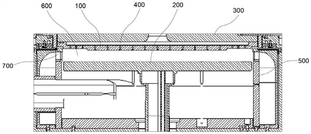
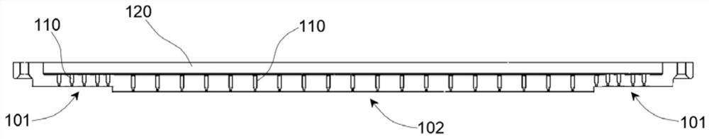
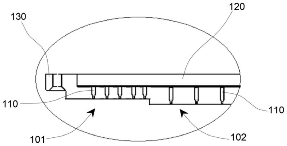
[0024] join Figure 1 to Figure 5 , the semiconductor process equipment includes a cavity 500 and a susceptor 200 disposed in the cavity 500 . A gas distribution device for semiconductor process equipment d...


PUM

PropertyMeasurementUnit
radiusaaaaaaaaaa

Abstract

The invention discloses semiconductor processing equipment and a gas distribution device thereof, and relates to the technical field of semiconductor processing equipment. The semiconductor process equipment comprises a cavity and a base arranged in the cavity. The gas distribution device comprises a gas distribution plate, and the gas distribution plate is arranged in the cavity and is opposite to the base. A plurality of gas distribution holes are formed in the gas distribution plate and are used for inputting process gas into the cavity; the side, facing the base, of the gas distribution plate is provided with a concave area and a convex area, the distance between the concave area and the base is a first distance, the distance between the convex area and the base is a second distance, and the first distance is larger than the second distance. According to the scheme, the concave area and the convex area enable the distance between each part in the gas distribution plate and the base to be different, so that the electric field between the gas distribution plate and the base is adjusted, the intensity of the electric field between the gas distribution plate and the base is more uniform, and the density of the insulating medium film is more uniform.

Description

technical field [0001] The invention relates to the technical field of semiconductor processing equipment, in particular to a semiconductor processing equipment and a gas distribution device thereof. Background technique [0002] With the development of semiconductor technology, the application of insulating dielectric films is becoming wider and wider. In the related art, the equipment for depositing an insulating dielectric film is used to deposit an insulating dielectric film by adding radio frequency power to ionize the process gas in the semiconductor device. In the related art, in order to avoid metal contamination in the equipment caused by the base electrode made of metal, a layer of ceramic is arranged between the base electrode and the wafer to isolate the base electrode made of metal. Because the charge on the surface of the ceramic layer used to isolate the base electrode cannot be guided away in time, there is a potential on the surface of the base, resulting i...

Claims


Application Information

Patent Timeline
Patent Type & Authority Applications(China)
IPC IPC(8): H01L21/67H01L21/687
CPCH01L21/67017H01L21/68785
Inventor 张文强郑波兰云峰秦海丰任晓艳王昊
Owner BEIJING NAURA MICROELECTRONICS EQUIP CO LTD
Why Eureka
Try Eureka