Silicon carbide Schottky diode and preparation method thereof
A Schottky diode, silicon carbide technology, applied in semiconductor/solid-state device manufacturing, electrical components, circuits, etc., can solve the problem of high electric field strength at the edge of the injection junction, low reverse withstand voltage of silicon carbide Schottky diode chips, and reliable It can improve the reverse withstand voltage and reliability, protect from damage, and improve uniformity.
- Summary
- Abstract
- Description
- Claims
- Application Information
AI Technical Summary
Problems solved by technology
Method used
Image

Examples
preparation example Construction
[0054] In addition, the present invention also provides a kind of preparation method of above-mentioned Schottky diode, comprises the following steps:
[0055] Rotate around the blind hole on one side of the substrate and perform ion implantation into the blind hole at the same time to form a P-type junction in the blind hole. During the ion implantation process, the angle between the direction of ion implantation and the substrate is an obtuse angle or acute angles.
[0056] The angle β between the direction of the ion implantation and the substrate is 75°-90°; preferably, the angle β between the direction of the ion implantation and the substrate is 75°.
[0057] The implantation energy of the ion implantation is 30-500KeV, the implantation temperature is 500-600°C, and the rotation angle α of the rotation is 0-270°. Preferably, the rotation angle α is 0°, 90°, 180°, or 270°.
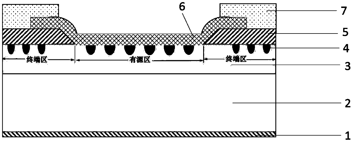
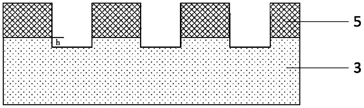
[0058] The depth h of the blind hole is 300-500nm;
[0059] The ions of the ion implantation ar...
Embodiment 1
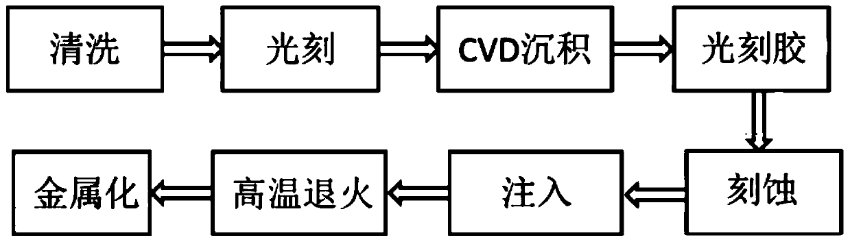
[0069] This embodiment provides a method for preparing a silicon carbide Schottky diode, such as figure 2 Shown is a process flow diagram of a method for preparing a silicon carbide Schottky diode, and the method specifically includes the following steps:
[0070] Cleaning lithography: cleaning the silicon carbide substrate 2 with the silicon carbide epitaxial layer 3, and then aligning and marking the patterns used in lithography on the silicon carbide epitaxial layer 3;
[0071] Making a mask layer: on the silicon carbide epitaxial layer 3, first make a first mask layer silicon dioxide layer by chemical vapor deposition, the thickness of the silicon dioxide layer is 2um; then on the first mask layer silicon dioxide Spin-coat positive photoresist on the layer as the second mask layer, perform pre-baking at 120°C, and expose under ultraviolet light;
[0072] Photolithography: photolithography is carried out on the above samples, and the pattern is photoetched onto the photor...
Embodiment 2
[0090] This embodiment provides a method for preparing a silicon carbide Schottky diode, such as figure 2 Shown is a process flow diagram of a method for preparing a silicon carbide Schottky diode, and the method specifically includes the following steps:
[0091] Cleaning lithography: cleaning the silicon carbide substrate 2 with the silicon carbide epitaxial layer 3, and then aligning and marking the patterns used in lithography on the silicon carbide epitaxial layer 3;
[0092] Make a mask layer: first make a first mask layer silicon dioxide layer on the silicon carbide epitaxial layer 3 by chemical vapor deposition, the thickness of the silicon dioxide layer is 2.5um; Spin-coat positive photoresist on the silicon layer as the second mask layer, perform prebaking at 120°C, and expose under ultraviolet light;
[0093] Photolithography: photolithography is carried out on the above samples, and the pattern is photoetched onto the photoresist of the second mask layer;
[009...
PUM
| Property | Measurement | Unit |
|---|---|---|
| Thickness | aaaaa | aaaaa |
Abstract
Description
Claims
Application Information
 - R&D
- Intellectual Property
- Life Sciences
- Materials
- Tech Scout
- Unparalleled Data Quality
- Higher Quality Content
- 60% Fewer Hallucinations
Browse by: Latest US Patents, China's latest patents, Technical Efficacy Thesaurus, Application Domain, Technology Topic, Popular Technical Reports.
© 2025 PatSnap. All rights reserved.Legal|Privacy policy|Modern Slavery Act Transparency Statement|Sitemap|About US| Contact US: help@patsnap.com