Supercharge Your Innovation With Domain-Expert AI Agents!

High efficiency micro device

A technology of efficiency and effect, applied in the field of high-efficiency micro-device

Pending Publication Date: 2022-03-08
VUEREAL INC
View PDF0 Cites 0 Cited by
  • Summary
  • Abstract
  • Description
  • Claims
  • Application Information

AI Technical Summary

Problems solved by technology

The challenge is the use of additional electrodes in small devices

Method used


Image

  • High efficiency micro device
  • High efficiency micro device

Examples


Embodiment Construction

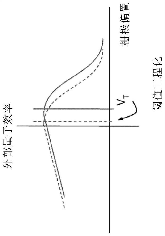
[0017] Integrating micro-optoelectronic devices into system substrates can provide high-performance and highly functional systems. To improve cost and produce higher pixel density devices, optoelectronic devices should be reduced in size. Examples of optoelectronic devices are, for example, sensors and light emitting devices such as light emitting diodes (LEDs). However, when reducing the size of these devices, device performance may start to degrade. Some reasons for reduced performance include, but are not limited to, higher leakage current due to defects, charge crowding at interfaces, unbalanced charges, and unwanted recombination, such as Auger and non-radiative recombination.

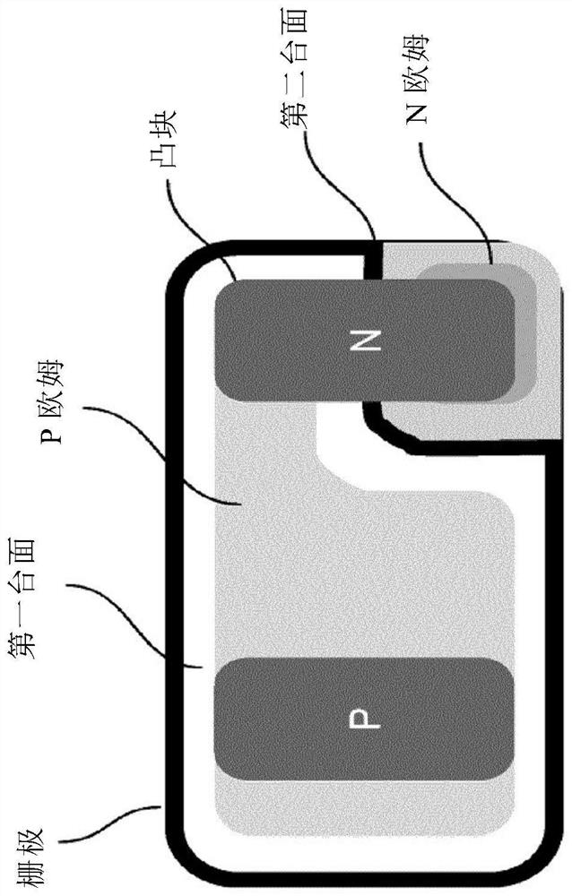
[0018] Various transfer and bonding methods can be used to transfer and bond the device layers to the system substrate. In one example, heat and pressure can be used to bond the device layer to the system substrate. In vertical solid-state devices, current flow in the vertical direction primari...


PUM


Abstract

A vertical solid state device includes: a connection pad; and a sidewall including a metal insulator semiconductor (MIS) structure; wherein a gate of the MIS structure is shorted to at least one contact of the vertical solid state device and a threshold voltage (VT) of the MIS structure is adjusted to improve efficiency of the device.

Description

technical field [0001] The present invention relates to vertical solid-state devices and methods of manufacturing the same. More particularly, the present invention relates to high efficiency microdevices. Background technique [0002] Sidewall defects are one of the main causes of performance degradation of microdevices. One approach to enhance performance is to use the gate to deactivate the activation defect by biasing the gate around the device. The challenge is the use of additional electrodes in small devices. Contents of the invention [0003] According to one embodiment, there is provided a vertical solid-state device comprising a p-contact, a p-doped layer, different functional layers (such as quantum wells, barriers, etc.), an n-doped layer, connection pads, and a metal-insulator-semiconductor (MIS ) sidewalls of the structure, wherein the gate of the MIS structure is shorted to at least one contact of the vertical solid state device. [0004] In another embo...

Claims


Application Information

Patent Timeline
Patent Type & Authority Applications(China)
IPC IPC(8): H01L21/8234H01L21/425H01L29/78
CPCH01L29/78H01L24/13H01L2224/13028H01L2224/13013H01L2224/14104H01L24/14H01L24/06H01L24/05H01L2224/0401H01L2224/05554H01L2224/05552H01L2224/06051H01L23/60H01L2924/12041H01L33/0037H01L2924/00012H01L33/04H01L33/06H01L33/0041H01L23/58H01L33/14H01L33/145
Inventor 戈尔拉玛瑞扎·恰吉埃桑诺拉·法蒂侯赛因·扎马尼·西博尼
Owner VUEREAL INC
Features
  • R&D
  • Intellectual Property
  • Life Sciences
  • Materials
  • Tech Scout
  • Unparalleled Data Quality
  • Higher Quality Content
  • 60% Fewer Hallucinations
Learn More