Reference voltage buffer for differential successive approximation register type ADC

A reference voltage buffer, voltage buffer technology, applied in the direction of instruments, electrical components, electrical signal transmission systems, etc., to achieve good transient characteristics, speed up the pull-down speed, reduce the effect of bias current

Pending Publication Date: 2022-03-15
SUZHOU UNIV
View PDF0 Cites 0 Cited by
  • Summary
  • Abstract
  • Description
  • Claims
  • Application Information

AI Technical Summary

Problems solved by technology

How to design the buffer with the least power consumption to provide the three reference voltages (positive reference voltage Vrp, negative reference voltage Vrn, and common-mode voltage Vcm) required by this differential structure is a key issue when designing a differential SAR ADC. Therefore, the power consumption of the reference voltage buffer tends to account for the majority of the overall power consumption of the SAR ADC

Method used


Image

  • Reference voltage buffer for differential successive approximation register type ADC
  • Reference voltage buffer for differential successive approximation register type ADC
  • Reference voltage buffer for differential successive approximation register type ADC

Examples


Embodiment

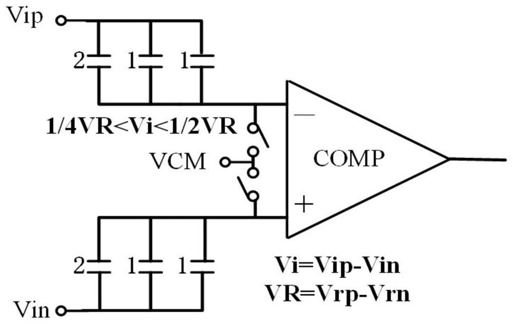
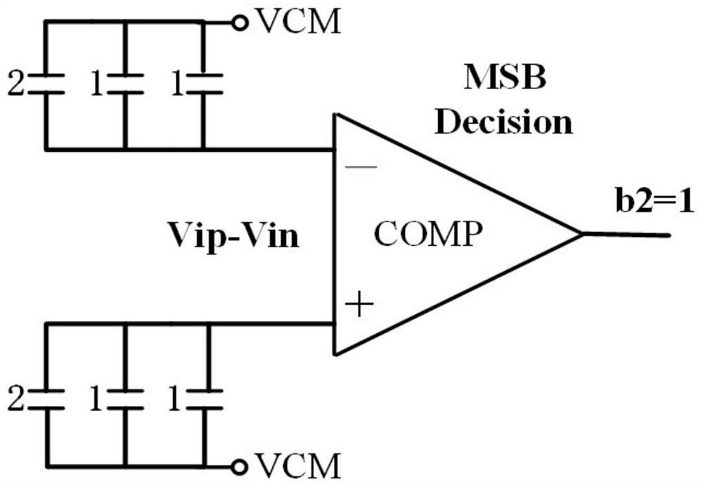
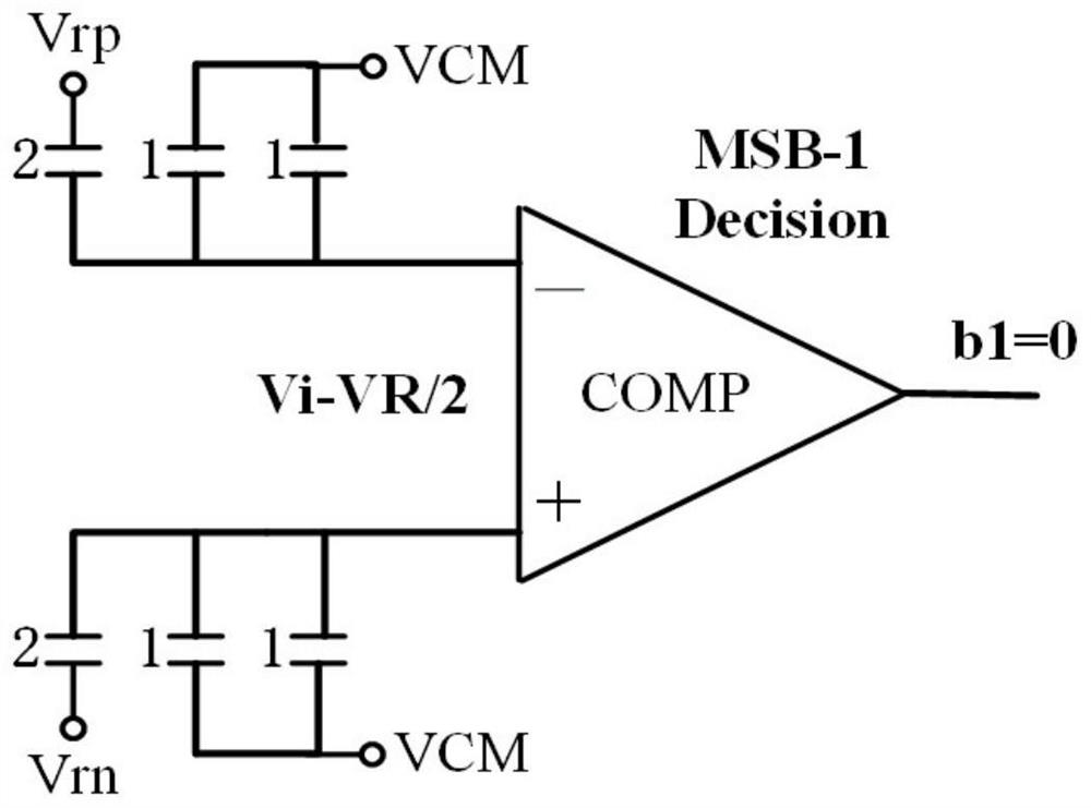
[0042] see Figure 5 As shown, this embodiment provides a reference voltage buffer for a differential successive approximation register type ADC, including an adjustable first voltage buffer, a second voltage buffer that generates a positive reference voltage Vrp, and a common-mode voltage a third voltage buffer of Vcm, wherein the bandgap reference voltage is output to the input of the second voltage buffer and the input of the third voltage buffer through the first voltage buffer;

[0043] The first voltage buffer includes a first error amplifier A1, a first PMOS transistor P1, a first resistor R1 and a second resistor R2;

[0044] The second voltage buffer includes a second error amplifier A2, a second PMOS transistor P2, a third resistor R3 and a fourth resistor R4;

[0045] The third voltage buffer includes a third error amplifier A3, a first NMOS transistor N1, a second NMOS transistor N2, a first current source I1 and a high voltage detector HD.

[0046] In one embodi...


PUM


Abstract

The invention discloses a reference voltage buffer for a differential successive approximation register type ADC (Analog to Digital Converter), which comprises a trimmable first voltage buffer, a second voltage buffer for generating a positive reference voltage Vrp and a third voltage buffer for generating a common-mode voltage Vcm, band-gap reference voltage is output to the input end of the second voltage buffer and the input end of the third voltage buffer through the first voltage buffer. The output voltage of the first voltage buffer can be changed by trimming the resistor R1, so that the output voltage of the second voltage buffer can be trimmed; and the third voltage buffer is pulled down in an accelerated manner through a high voltage detector (HD), so that Vcm can be quickly established with very low bias current. The requirement for low power consumption of the first voltage buffer and the requirement for accurate trimming are consistent; meanwhile, the second voltage buffer needs accurate output voltage, and the third voltage buffer does not need accurate output voltage. The on-chip reference voltage buffer can well meet the requirement of a differential SAR type ADC for the on-chip reference voltage buffer.

Description

technical field [0001] The invention relates to the technical field of integrated circuit design, in particular to a buffer for providing a series of reference voltages for a high-precision full differential successive approximation register ADC. Background technique [0002] The analog-to-digital converter (Analog-to-Digital Converter, ADC) is a bridge between the real world and the digital world. The successive approximation register (Successive Approximation Register, SAR) structure is very suitable for realizing medium-speed and medium-high-precision ADCs. Compact structure, low power consumption, and the ability to benefit from manufacturing process advancements. [0003] Figures 1 to 4 Taking 3 bits as an example, the quantization process of the differential SAR ADC is illustrated, where, figure 1 is the sampling phase state, figure 2 For the first comparison to get b2, image 3 Get b1 for the second comparison, Figure 4 Get b0 for the third comparison. This k...

Claims


Application Information

Patent Timeline
IPC IPC(8): H03M1/38
CPCH03M1/38
Inventor 白春风汤雁婷徐祥
Owner SUZHOU UNIV
Why Eureka
Try Eureka