
Sensing and calculating integrated single-photon imaging chip and method

An imaging chip, single-photon technology, applied in the field of electronics, can solve problems such as increasing the power consumption of single-photon arrays, high power consumption restricting application scenarios, etc., to achieve high frame rate perception and calculation, high parallelism, and improved calculation rate. Effect

Pending Publication Date: 2022-03-18
FUDAN UNIV
View PDF0 Cites 3 Cited by
  • Summary
  • Abstract
  • Description
  • Claims
  • Application Information

AI Technical Summary

Problems solved by technology

To ensure the above-mentioned high data rate, multiple parallel high-speed output buffers need to be designed for the single photon array, which will greatly increase the power consumption of the single photon array
At the same time, the back-end processing chip must also have high-bandwidth, high-speed data reading capabilities, and high-speed real-time processing capabilities for multi-channel serial input data. The avoided high power consumption also severely limits the application scenarios

Method used


Image

  • Sensing and calculating integrated single-photon imaging chip and method
  • Sensing and calculating integrated single-photon imaging chip and method
  • Sensing and calculating integrated single-photon imaging chip and method

Examples


Embodiment Construction

[0035] The present invention will be described in detail below in conjunction with the accompanying drawings and specific embodiments. This embodiment is carried out on the premise of the technical solution of the present invention, and detailed implementation and specific operation process are given, but the protection scope of the present invention is not limited to the following embodiments.

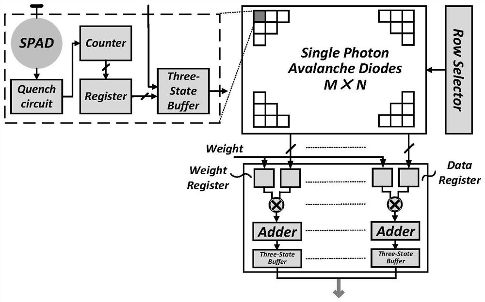
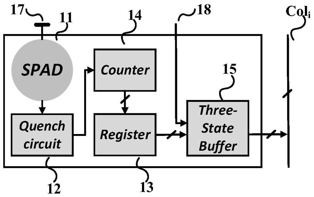
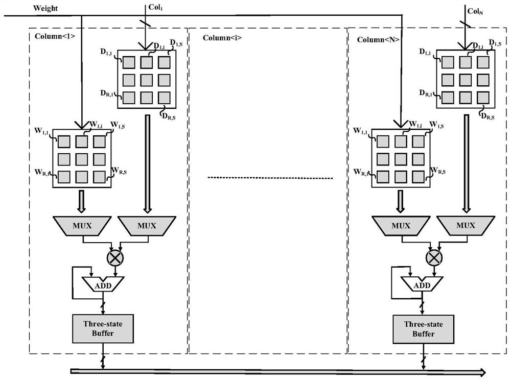
[0036] A sensor-computing integrated single-photon imaging chip, such as Figure 1 to Figure 6 As shown, it includes a single-photon photosensitive counting array, a convolution calculation column processing circuit, a row selection circuit, a convolution weight read-write circuit, a column bus and an output bus. The single-photon photosensitive counting array consists of single-photon pixel circuits with M rows and N columns Arranged, M and N are integers greater than 1, there are N column buses, M pulse output terminals of the row selection circuit, and the single-photon pixel circu...


PUM


Abstract

The invention relates to a sensing and calculation integrated single-photon imaging chip and method, and the chip mainly consists of a single-photon photosensitive counting array, a convolution calculation column processing circuit, a row selection circuit and the like. A convolution weight is written into a column processing circuit in advance, pixels of a chip array count the number of photons and register the number of photons in the pixels, a sequential control circuit transmits photon data in the chip array to the column processing circuit row by row, the photon data and the pre-stored convolution weight are multiplied and added, and the photon data in the chip array are stored in the column processing circuit. Therefore, the convolution calculation of the array photon image and the convolution kernel weight is realized. According to the chip, a convolution calculation function is fused in a traditional single-photon imaging architecture, and the chip has the characteristic of integration of sensing and calculation. The chip can quickly extract weak image features and greatly compress the output single-photon imaging data volume.

Description

technical field [0001] The invention relates to the field of electronic technology, in particular to a sensor-computing integrated single-photon imaging chip and method. Background technique [0002] Single photon detectors can count individual photons and have imaging capabilities in extremely weak signal scenarios. The pixels of a single photon detector array usually include single photon devices, quenching circuits, counters and registers. The single-photon device works in the Geiger mode. When the photon emitted by the target is received, the device undergoes a Geiger avalanche. The quenching circuit quickly adjusts the bias voltage at both ends of the single-photon device to make the single-photon device exit the avalanche. At the same time, the quenching circuit outputs a Represents the pulse signal of photon detection, the pulse signal enters the counter, and the counter data is incremented by 1. After the single-photon device exits the avalanche, it waits for a cer...

Claims


Application Information

Patent Timeline
IPC IPC(8): G01J1/44G06F17/15
CPCG01J1/44G06F17/15G01J2001/442Y02D10/00
Inventor 黄张成陈迟晓刘琦
Owner FUDAN UNIV
Learn More