Optical chip structure of high-power semiconductor laser, preparation method of optical chip structure and laser
A technology of optical chips and semiconductors, applied in the field of lasers, to achieve ultra-high laser power output and improve the effect of laser output power
- Summary
- Abstract
- Description
- Claims
- Application Information
AI Technical Summary
Problems solved by technology
Method used
Image

Examples
Embodiment Construction
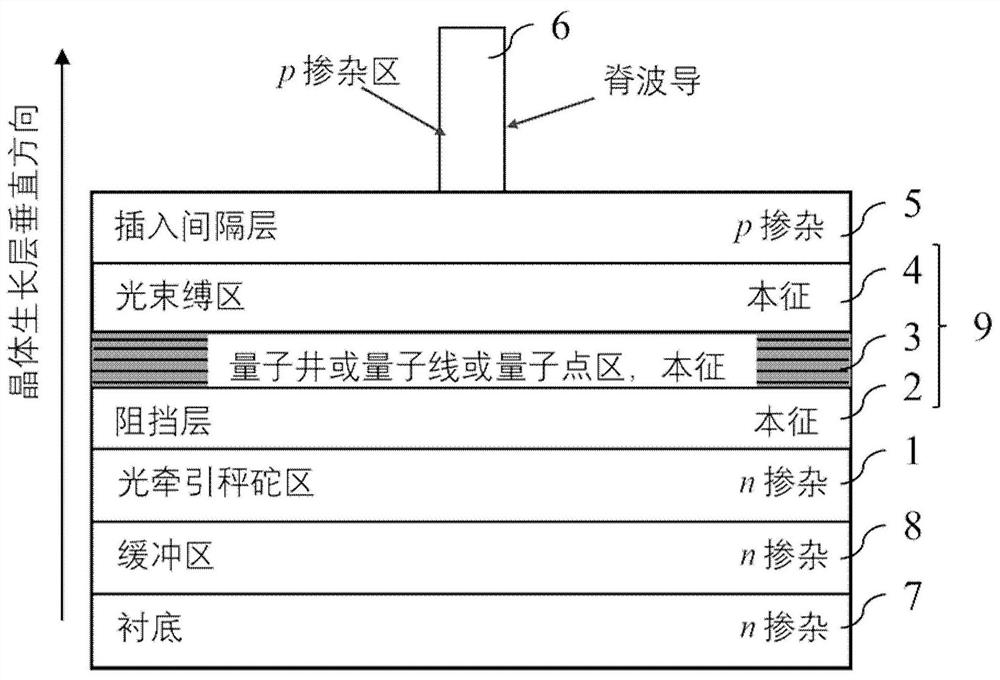
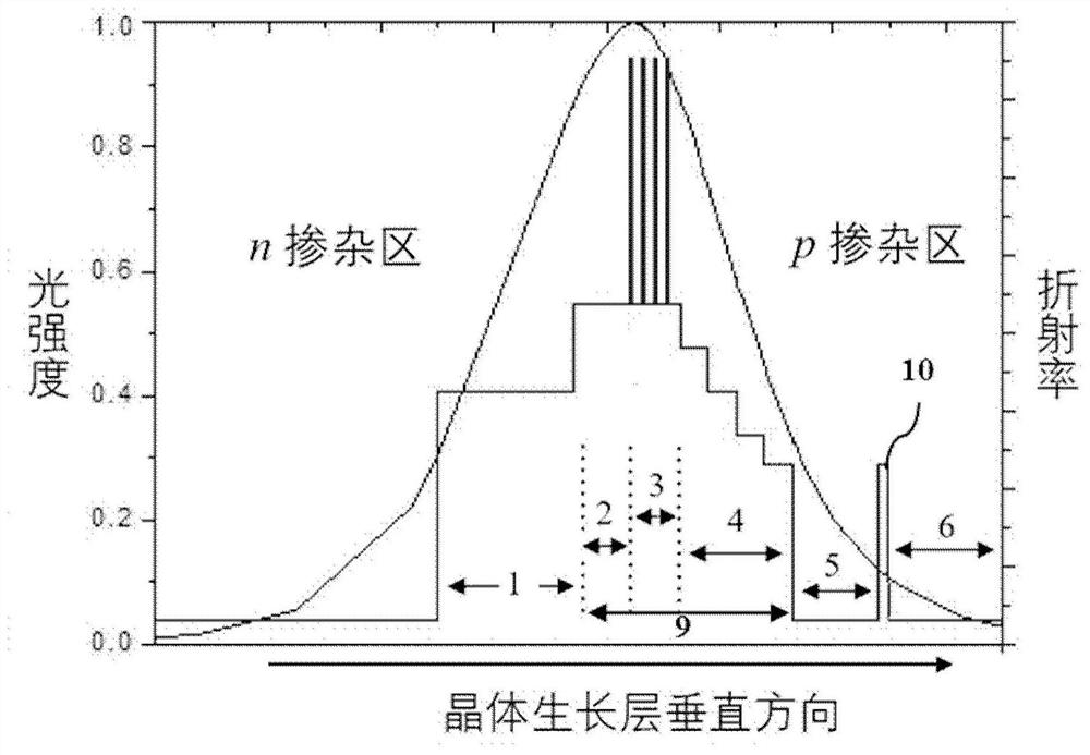
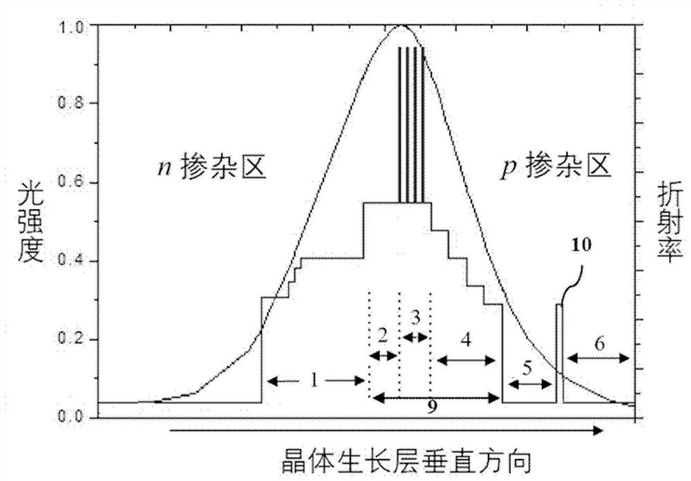
[0029] In order to make the object, technical solution and advantages of the present invention clearer, the present invention will be described in further detail below in conjunction with specific embodiments and with reference to the accompanying drawings.
[0030] It should be noted that, in the accompanying drawings or in the text of the specification, implementations that are not shown or described are forms known to those of ordinary skill in the art, and are not described in detail. In addition, the above definitions of each element and method are not limited to the various specific structures, shapes or methods mentioned in the embodiments, and those skilled in the art can easily modify or replace them.
[0031] It should also be noted that the directional terms mentioned in the embodiments, such as "up", "down", "front", "back", "left", "right", etc., are only referring to the directions of the drawings, not Used to limit the protection scope of this disclosure. Throu...
PUM
 Abstract
Description
Claims
Application Information