Manufacturing method of film bulk acoustic resonator
A thin-film bulk acoustic wave and manufacturing method technology, applied in electrical components, impedance networks, etc., can solve the problems of inability to meet high-performance radio frequency systems, the quality factor cannot be further improved, and the structural strength is not enough, so as to avoid high-frequency coupling problems, The effect of eliminating boundary clutter and improving mechanical strength
- Summary
- Abstract
- Description
- Claims
- Application Information
AI Technical Summary
Problems solved by technology
Method used
Image

Examples
Embodiment 1
[0029] Embodiment 1 of the present invention provides a method for manufacturing a thin film bulk acoustic resonator, the method comprising:
[0030] S01: providing a first substrate; forming a cavity on the upper surface of the first substrate;
[0031] S02: forming a sacrificial layer in the cavity;
[0032] S03: sequentially forming a stacked first electrode, a piezoelectric layer, and a second electrode on the first substrate and on the sacrificial layer;
[0033] S04: At least one of the first electrode and the second electrode has an annular arched bridge, the annular arched bridge is raised away from the piezoelectric layer, and the inner surface of the annular arched bridge forms a ring void;
[0034] S05: removing the sacrificial layer.
[0035] It should be noted that the step S0N does not represent a sequence.
[0036] Figure 1 to Figure 7 It is a structural diagram corresponding to each step of the manufacturing method of the thin film bulk acoustic resonator ...
Embodiment 2
[0051] Figure 8 to Figure 15 It is a structural diagram corresponding to each step of the manufacturing method of the thin film bulk acoustic resonator in this embodiment. Please refer below Figure 8 to Figure 15 The manufacturing method of the thin film bulk acoustic resonator will be described. The difference between this embodiment and Embodiment 1 is that in this embodiment, the first electrode 101 is also formed with an annular arched bridge.
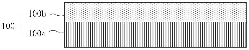
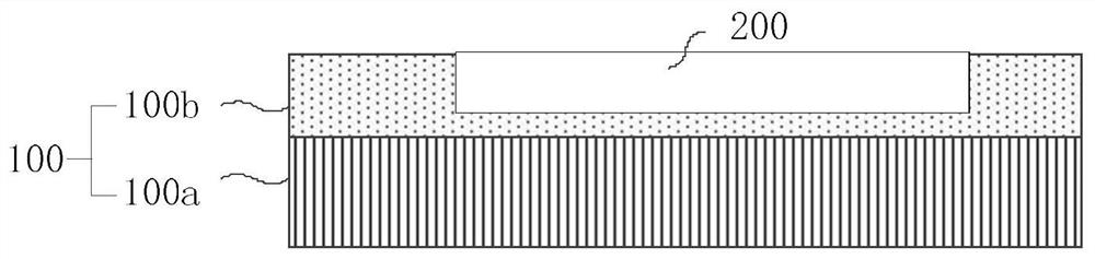
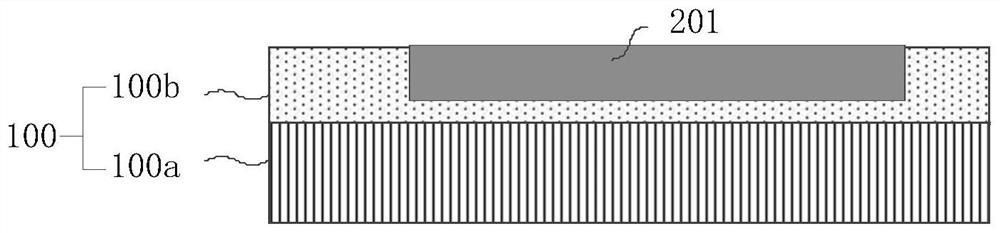
[0052] refer to Figure 8 with Figure 9 , providing a first substrate 100, the first substrate 100 is a double-layer structure, including a base 100a and a supporting layer 100b on the base 100a. A cavity 200 is formed on the upper surface of the first substrate 100 through an etching process, and a sacrificial layer 201 is formed in the cavity. For the materials, structures, and methods involved in the above steps, refer to the relevant description of Embodiment 1, and will not be repeated here.
[0053] refer to Figure...
Embodiment 3
[0060] Figure 16 to Figure 19 It is a structural diagram corresponding to each step of the manufacturing method of the thin film bulk acoustic resonator in this embodiment. Please refer below Figure 16 to Figure 19 The manufacturing method of the thin film bulk acoustic resonator will be described. In this embodiment, a groove 40 is formed in the piezoelectric layer 102 .
[0061] refer to Figure 16 , in this embodiment, the steps before forming the piezoelectric layer 102 are the same as in Embodiment 2, and the relevant steps refer to Embodiment 2, and the drawings refer to Figure 8 to Figure 13 , after forming the piezoelectric layer 102, refer to Figure 16 , forming a trench 40 in the piezoelectric layer 102 . The trench 40 may be formed through a dry etching process. In this embodiment, the trench 40 is a closed ring and penetrates the piezoelectric layer 102 to expose the second sacrificial layer below the piezoelectric layer 102 . The inner sidewall of the tr...
PUM
 Abstract
Description
Claims
Application Information
 - R&D Engineer
- R&D Manager
- IP Professional
- Industry Leading Data Capabilities
- Powerful AI technology
- Patent DNA Extraction
Browse by: Latest US Patents, China's latest patents, Technical Efficacy Thesaurus, Application Domain, Technology Topic.
© 2024 PatSnap. All rights reserved.Legal|Privacy policy|Modern Slavery Act Transparency Statement|Sitemap