Film bulk acoustic resonator, manufacturing method thereof and filter
A thin-film bulk acoustic wave and resonator technology, which is applied to electrical components, impedance networks, etc., can solve the problems that cannot meet the requirements of high-performance radio frequency systems, and the quality factor cannot be further improved, so as to achieve improved conductivity, good structural stability, and improved accuracy. sexual effect
- Summary
- Abstract
- Description
- Claims
- Application Information
AI Technical Summary
Problems solved by technology
Method used
Image

Examples
Embodiment 1
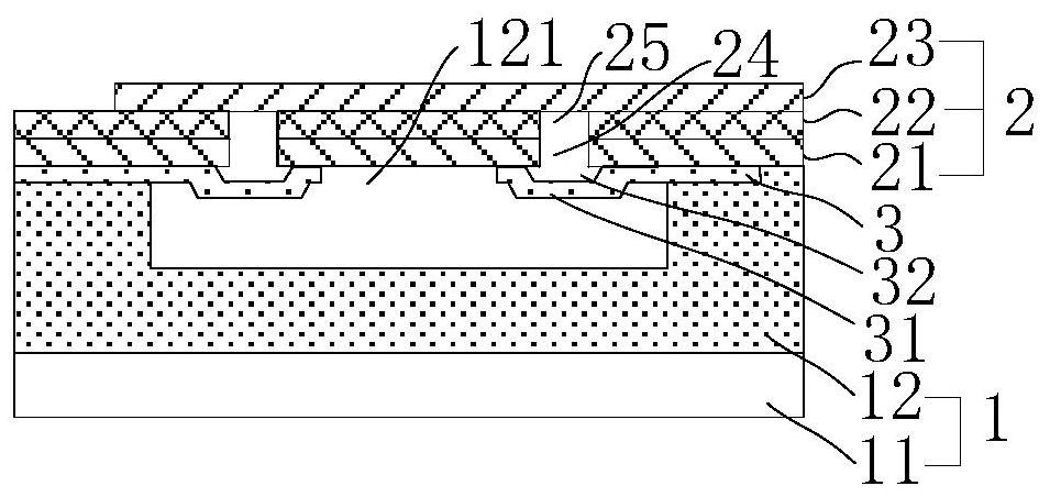
[0050] Embodiment 1 provides a thin film bulk acoustic resonator, figure 1 For a schematic cross-sectional structure diagram of a thin film bulk acoustic resonator provided in Embodiment 1 of the present invention, please refer to figure 1 , the thin film bulk acoustic resonator consists of:
[0051] The piezoelectric stack structure 2, the piezoelectric stack structure 2 includes a first electrode 21, a piezoelectric layer 22, and a second electrode 23 stacked sequentially from bottom to top, at least one of the first electrode 21 and the second electrode 23 has an annular groove 24 running through the corresponding electrode;
[0052] The electrode lead-out structure 3 is provided on the corresponding electrode provided with the annular groove 24, the electrode lead-out structure 3 covers at least part of the ring-shaped groove 24 and extends to the invalid resonance area, and the electrode lead-out structure 3 includes a protruding direction away from the piezoelectric lay...
Embodiment 2
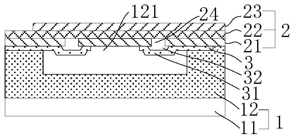
[0069] Embodiment 2 provides a thin film bulk acoustic resonator, figure 2 It is a schematic cross-sectional structure diagram of a thin film bulk acoustic resonator in Embodiment 2 of the present invention. The difference between this embodiment and Embodiment 1 is that the piezoelectric layer 22 in Embodiment 1 is provided with a first groove 25, and in Embodiment 2 The piezoelectric layer 22 is a complete film layer, specifically: the piezoelectric layer 22 is a complete film layer, covers the first cavity 121 and extends to the first substrate 1 outside the first cavity 121 . The piezoelectric layer 22 is complete without being etched, which can ensure the structural strength of the resonator and improve the yield of the resonator. Other structural features of the thin film bulk acoustic resonator in this embodiment are the same as those in Embodiment 1, and will not be repeated here.
Embodiment 3
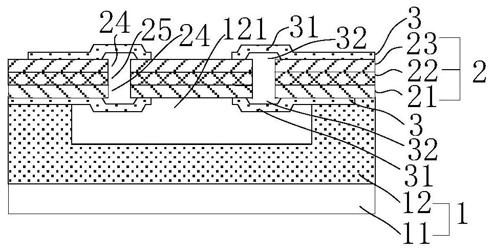
[0071] Embodiment 3 provides a thin film bulk acoustic resonator, image 3 It is a schematic cross-sectional structure diagram of a thin film bulk acoustic resonator according to Embodiment 3 of the present invention. The difference between this embodiment and Embodiment 1 is that the electrode lead-out structure 3 in Embodiment 1 is only provided on the first electrode 21 or the second electrode 23 , the electrode lead-out structure in Embodiment 3 is disposed on the first electrode 21 and the second electrode 23 . Specifically:
[0072] In this embodiment, both the first electrode 21 and the second electrode 24 are provided with an electrode lead-out structure 3, and the electrode lead-out structure arranged on the first electrode 21 and the electrode lead-out structure arranged on the second electrode 23 respectively have a structure extending to The second part outside the effective resonance area, the second part is used as the electrode connection end. In addition, the...
PUM
 Abstract
Description
Claims
Application Information
 - R&D Engineer
- R&D Manager
- IP Professional
- Industry Leading Data Capabilities
- Powerful AI technology
- Patent DNA Extraction
Browse by: Latest US Patents, China's latest patents, Technical Efficacy Thesaurus, Application Domain, Technology Topic.
© 2024 PatSnap. All rights reserved.Legal|Privacy policy|Modern Slavery Act Transparency Statement|Sitemap