Manufacturing method of film bulk acoustic resonator and filter

A thin-film bulk acoustic wave and manufacturing method technology, applied in the direction of electrical components, impedance networks, etc., can solve the problems that the quality factor cannot be further improved, cannot meet the high-performance radio frequency system, etc., and achieve improved conductivity, improved accuracy, and good structural stability sexual effect

Pending Publication Date: 2022-03-29
NINGBO SEMICON INT CORP
View PDF0 Cites 0 Cited by
  • Summary
  • Abstract
  • Description
  • Claims
  • Application Information

AI Technical Summary

Problems solved by technology

[0004] However, the quality factor (Q) of the cavity-type thin-film bulk acoustic resonator produced at present cannot be further improved, so it cannot meet the needs of high-performance radio frequency systems

Method used


Image

  • Manufacturing method of film bulk acoustic resonator and filter
  • Manufacturing method of film bulk acoustic resonator and filter
  • Manufacturing method of film bulk acoustic resonator and filter

Examples


Embodiment 1

[0034] figure 1 It is a flow chart of the manufacturing method of the thin film bulk acoustic resonator according to Embodiment 1 of the present invention, referring to figure 1 , embodiment 1 provides a kind of manufacturing method of thin film bulk acoustic resonator, the manufacturing method of thin film bulk acoustic resonator comprises:

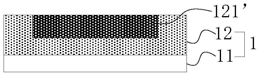
[0035] S01: forming a first substrate having a first sacrificial layer;

[0036] S02: sequentially forming a first electrode, forming a piezoelectric layer, and forming a second electrode on the first substrate, the first electrode covering the first sacrificial layer;

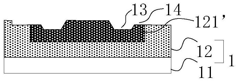
[0037] S03: Form an annular groove through the corresponding electrode on at least one of the first electrode and the second electrode; form an electrode lead-out structure with an arched bridge structure on the corresponding electrode formed with the annular groove, the arched bridge structure and The annular groove is opposite;

[0038] S04: removing the first sacri...

Embodiment 2

[0066] Embodiment 2 provides a method for manufacturing a thin film bulk acoustic resonator, Figure 7 It is a schematic structural diagram of a thin film bulk acoustic resonator manufactured according to the manufacturing method of a thin film bulk acoustic resonator in this embodiment. The difference between this embodiment and Embodiment 1 is that the piezoelectric layer 22 in Embodiment 1 is formed with a first groove 25. The piezoelectric layer 22 in this embodiment is a complete film layer, the step of etching the piezoelectric layer 22 in the above-mentioned embodiment 1 is omitted, and the remaining steps refer to the above-mentioned embodiment 1. Specifically: the piezoelectric layer 22 is not etched, it is a complete film layer, covers the first cavity 121 and extends to the first substrate 11 outside the first cavity 121, so as to ensure the structural strength of the resonator and improve Resonator yield.

Embodiment 3

[0068] Embodiment 3 provides a method for manufacturing a thin film bulk acoustic resonator. The difference between this embodiment and Embodiment 1 is that electrode lead-out structures are formed on both the first electrode 21 and the second electrode 23 in Embodiment 1. Embodiment 3 In 3, the electrode lead-out structure is only formed on the first electrode 21 or the second electrode 23 . When the electrode lead-out structure is formed on the first electrode 21, the step of forming the second electrode lead-out structure 4 on the second electrode 23 in Embodiment 1 can be omitted; when the electrode lead-out structure is formed on the second electrode 23, it can be The step of forming the first electrode lead-out structure 3 on the first electrode 21 in Embodiment 1 is omitted. The structure of the film bulk acoustic resonator will be described below by taking the formation of the first electrode lead-out structure 3 on the first electrode 21 as an example. The formation m...


PUM


Abstract

The invention relates to a manufacturing method of a film bulk acoustic resonator and a filter. The manufacturing method comprises the following steps: forming a first substrate with a first sacrificial layer; sequentially forming a first electrode, a piezoelectric layer and a second electrode, wherein the first electrode covers the first sacrificial layer; forming an annular groove penetrating through the corresponding electrode on at least one of the first electrode and the second electrode; forming an electrode leading-out structure with an arched bridge structure on the corresponding electrode with the annular groove, wherein the arched bridge structure is opposite to the annular groove; and removing the first sacrificial layer to form a first cavity. According to the invention, the boundary of the effective resonance area is defined through the area where the annular gap of the electrode extraction structure is located, and the end part of the corresponding electrode at the boundary of the effective resonance area is in contact with the gas in the gap through the annular groove, so that the effect of eliminating the boundary clutter of the electrode in the effective resonance area is achieved, and the Q value of the resonator is improved.

Description

technical field [0001] The invention relates to the field of semiconductor device manufacturing, in particular to a method for manufacturing a thin-film bulk acoustic wave resonator and a filter. Background technique [0002] Since the development of analog RF communication technology in the early 1990s, RF front-end modules have gradually become the core components of communication equipment. Among all RF front-end modules, filters have become the components with the strongest growth momentum and the greatest development prospects. With the rapid development of wireless communication technology and the maturity of 5G communication protocols, the market has also put forward stricter standards for the performance of RF filters in all aspects. The performance of a filter is determined by the resonator units that make up the filter. Among the existing filters, the film bulk acoustic resonator (FBAR) has the characteristics of small size, low insertion loss, large out-of-band ...

Claims


Application Information

Patent Timeline
Patent Type & Authority Applications(China)
IPC IPC(8): H03H3/02H03H9/02H03H9/64
CPCH03H3/02H03H9/02H03H9/64
Inventor 黄河
Owner NINGBO SEMICON INT CORP
Why Eureka
Try Eureka