Circuit and method for shortening pixel output stabilization time
An output stability and time technology, applied in the field of image sensors, can solve the problems of reducing the dynamic range of pixels, reducing the output voltage of pixels, affecting the dynamic range of the chip, etc., to shorten the stabilization time, increase the output frame rate, and shorten the required time.
- Summary
- Abstract
- Description
- Claims
- Application Information
AI Technical Summary
Problems solved by technology
Method used
Image
Examples
Embodiment 1
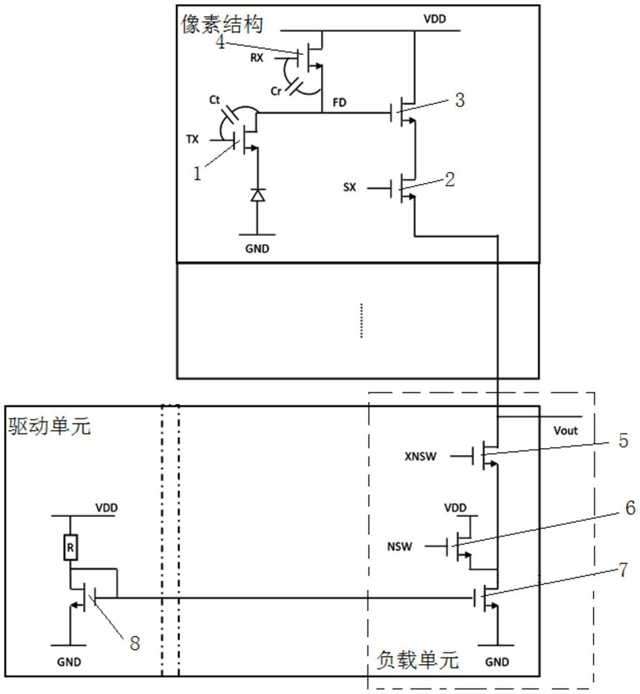
[0036]This embodiment discloses a circuit for shortening the pixel output stabilization time. The circuit includes a drive unit (1), a load unit (N) and a pixel unit (M rows and N columns); the pixel unit is composed of a pixel matrix with M rows and N columns ; Each row of pixels corresponds to a load unit (N load units); as figure 1 As shown, each load unit includes a first MOS transistor 5 and a second MOS transistor 6, and the first MOS transistor 5 is used to cut off the tail current provided by the pixel unit during the period of electronic reading of the third MOS transistor 1 Signal; the second MOS transistor 6 is used to control the load MOS transistor 7 to work normally during the period of electronic reading of the third MOS transistor 1 .
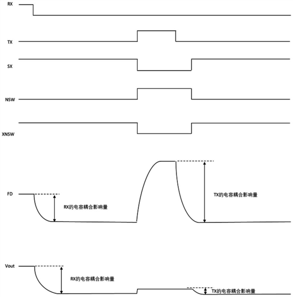
[0037] The load unit set in this embodiment can provide a stable tail current for the pixel unit by controlling the phase relationship of the control signals of the first MOS transistor 5, the second MOS transistor 6, the fourth...
Embodiment 2
[0048] This embodiment discloses a method for shortening the pixel output stabilization time. This embodiment is to realize the circuit for shortening the pixel output stabilization time provided in Embodiment 1. The method steps include:
[0049] By closing the fourth MOS transistor 2 and the first MOS transistor 5, the tail current signal of the pixel unit is cut off, and under the control of the second MOS transistor 6, a voltage signal is provided to the load MOS transistor 7;
[0050] Applying a voltage signal to the third MOS transistor 1, and reading the pixel signal in the pixel unit;
[0051] After the pixel signal reading is completed, stop the voltage signal applied to the third MOS transistor 1;
[0052] And turn on the fourth MOS transistor 2 and the first MOS transistor 5 to provide the tail current signal to the pixel unit, and cut off the voltage signal provided to the load unit under the control of the second MOS transistor 6 .
[0053] exist figure 1 The si...
Embodiment 3
[0058] This embodiment discloses an image sensor, including a pixel array; the pixel array includes a number of circuits for shortening the pixel output stabilization time as in Embodiment 1, and the circuits for shortening the pixel output stabilization time are uniform in the form of an array arranged.
[0059] In the image sensor provided in this embodiment, the other parts that make up the image sensor are the parts of the CMOS image sensor in the prior art, but the timing control circuit provided by the embodiment one is used in the part of the pixel array, which can make the image sensor It is faster and more stable when outputting image quality.
PUM
 Abstract
Description
Claims
Application Information

