Chip architecture and signal integrity test method

A signal integrity and chip technology, used in digital circuit testing, electronic circuit testing, architecture with a single central processing unit, etc., can solve the problem caused by the inability to determine the signal integrity of the chip, the inability to check whether there is a problem inside the chip, and the inability to adjust problems such as external motherboard links, to achieve the effect of low test cost, ensure signal integrity, and simple and fast process

Pending Publication Date: 2022-04-08
山东云海国创云计算装备产业创新中心有限公司
View PDF0 Cites 1 Cited by
  • Summary
  • Abstract
  • Description
  • Claims
  • Application Information

AI Technical Summary

Problems solved by technology

This test method relies on the mutual support between the motherboard and the chip, but since the range of the communication link obviously extends beyond the scope of the original chip, even if there is a problem with the communication link, it is impossible to de

Method used


Image

  • Chip architecture and signal integrity test method
  • Chip architecture and signal integrity test method
  • Chip architecture and signal integrity test method

Examples


Embodiment Construction

[0045] The following will clearly and completely describe the technical solutions in the embodiments of the present invention with reference to the accompanying drawings in the embodiments of the present invention. Obviously, the described embodiments are only some, not all, embodiments of the present invention. Based on the embodiments of the present invention, all other embodiments obtained by persons of ordinary skill in the art without making creative efforts belong to the protection scope of the present invention.

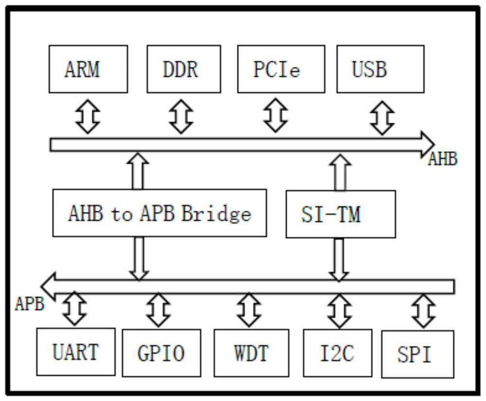
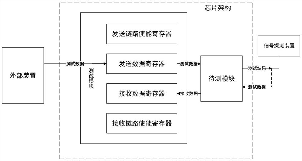
[0046] Signal integrity testing is different from wafer testing and FT testing. Generally, the entire link is tested during chip operation after the chip is installed on the motherboard. This test method relies on the mutual support between the motherboard and the chip, but since the range of the communication link obviously extends beyond the scope of the original chip, even if there is a problem with the communication link, it is impossible to determine wheth...


PUM


Abstract

The invention discloses a chip architecture and a signal integrity test method.The chip architecture comprises a plurality of modules to be tested and a test module, the test module comprises a function register, a data register and a state register, and when the test module receives a test instruction of a communication link of any one module to be tested, the function register is connected with the data register; and configuring the function register and the data register corresponding to the test instruction according to the test instruction, so that the state register and/or the pin of the to-be-tested module output a test result. The chip does not need to be installed on a mainboard, the signal test result of the communication link of each to-be-tested module can be obtained directly according to the test module in the chip architecture, the process is simple and rapid, the test cost is low, the test range is clear, the test effects of different to-be-tested modules can be accurately and rapidly determined, and the test efficiency is improved. And the signal integrity of the chip is ensured.

Description

technical field [0001] The invention relates to the field of chip testing, in particular to a chip architecture and a signal integrity testing method. Background technique [0002] At present, chip testing usually includes wafer wafer testing and FT (Final Test) after chip packaging, including current testing, voltage testing, functional testing, timing testing, etc., while signal integrity testing is different from wafer testing. Test and FT test, generally after the chip is installed on the main board, the whole link is tested during the operation of the chip. This test method relies on the mutual support between the motherboard and the chip, but since the range of the communication link obviously extends beyond the scope of the original chip, even if there is a problem with the communication link, it is impossible to determine whether the problem of the link is caused by the signal integrity of the chip. Due to the nature of the chip, it is impossible to check whether th...

Claims


Application Information

Patent Timeline
IPC IPC(8): G06F15/78G01R31/317G01R31/319
Inventor 庄戌堃
Owner 山东云海国创云计算装备产业创新中心有限公司
Why Eureka
Try Eureka