Display panel, display module and mobile terminal
A display panel and display module technology, which is applied in the direction of electrical components, electrical solid devices, circuits, etc., can solve the problems of carbon dust and other problems, and achieve the effect of improving cleanliness and avoiding residues
- Summary
- Abstract
- Description
- Claims
- Application Information
AI Technical Summary
Problems solved by technology
Method used
Image

Examples
Embodiment Construction
[0037] The technical solutions in the embodiments of the present application will be clearly and completely described below in conjunction with the drawings in the embodiments of the present application. Apparently, the described embodiments are only some of the embodiments of this application, not all of them. Based on the embodiments in this application, all other embodiments obtained by those skilled in the art without making creative efforts belong to the scope of protection of this application.
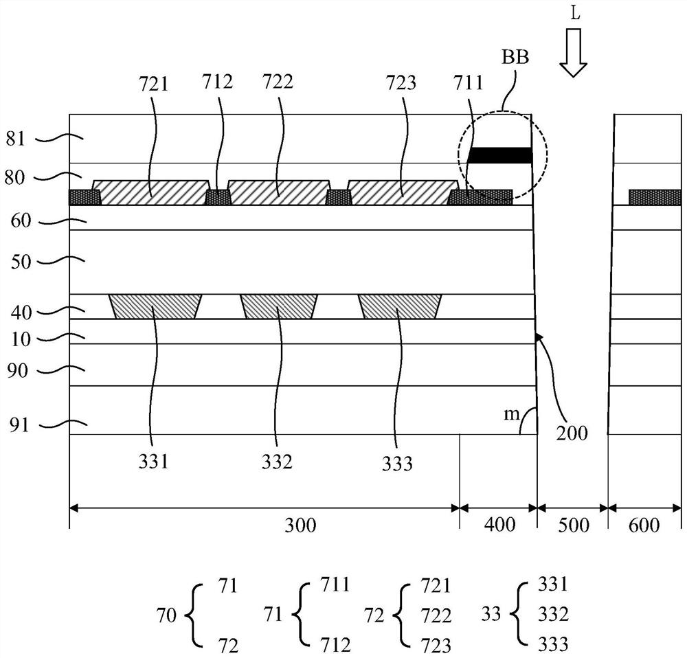
[0038] see figure 1 , figure 1 It is the film layer structure diagram after cutting of the existing display panel. In the existing OLED display panel, in order to reduce the thickness of the display panel, it can use the depolarizer technology to make the OLED panel, that is, replace the existing polarizer with the color resist layer and the black matrix layer, and in order to ensure the flatness of the product, It usually coats a first flat layer on the color filter layer, an...
PUM
| Property | Measurement | Unit |
|---|---|---|
| Angle range | aaaaa | aaaaa |
Abstract
Description
Claims
Application Information
 - Generate Ideas
- Intellectual Property
- Life Sciences
- Materials
- Tech Scout
- Unparalleled Data Quality
- Higher Quality Content
- 60% Fewer Hallucinations
Browse by: Latest US Patents, China's latest patents, Technical Efficacy Thesaurus, Application Domain, Technology Topic, Popular Technical Reports.
© 2025 PatSnap. All rights reserved.Legal|Privacy policy|Modern Slavery Act Transparency Statement|Sitemap|About US| Contact US: help@patsnap.com