
Test method of memory device implemented in multi-chip package (MCP) and method of manufacturing MCP including test method

A chip mounting and memory controller technology, applied in semiconductor/solid-state device testing/measurement, information storage, static memory, etc., can solve the problems of reduced productivity of MCP testing

Pending Publication Date: 2022-04-12
SAMSUNG ELECTRONICS CO LTD
View PDF8 Cites 0 Cited by
  • Summary
  • Abstract
  • Description
  • Claims
  • Application Information

AI Technical Summary

Problems solved by technology

Therefore, the productivity of MCP testing may be reduced

Method used


Image

  • Test method of memory device implemented in multi-chip package (MCP) and method of manufacturing MCP including test method
  • Test method of memory device implemented in multi-chip package (MCP) and method of manufacturing MCP including test method
  • Test method of memory device implemented in multi-chip package (MCP) and method of manufacturing MCP including test method

Examples


Embodiment Construction

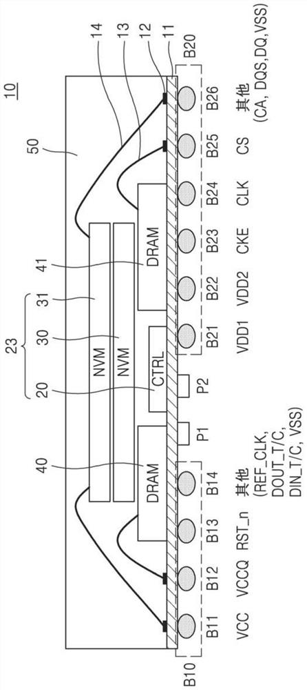
[0025] figure 1 is a diagram illustrating an example of implementing a memory device in a multi-chip package (MCP) 10 according to an embodiment of the inventive concept. Hereinafter, the terms "MCP 10" and "storage device 10" may be used interchangeably.

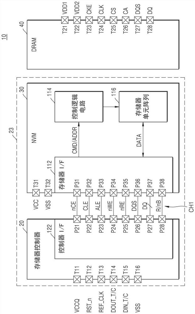
[0026] refer to figure 1 , the MCP 10 includes a package substrate 11, a memory controller chip 20, non-volatile memory (NVM) chips 30 and 31, DRAM chips 40 and 41, first wires 13, second wires 14, external connection terminals B11 to B14, P1 and P2 and B21 to B26 , and the molding layer 50 . Here, the external connection terminals B11 to B14, P1 and P2, and B21 to B26 may be referred to as package terminals or package balls. exist figure 1 In the MCP 10, two NVM chips 30 and 31 and two DRAM chips 40 and 41 are shown, but the inventive concept is not limited thereto, and other configurations are also possible. For example, MCP 10 can include 2 n NVM chips (n is a natural number equal to or greater than 0) and one or m...


PUM


Abstract

A method of manufacturing a multi-chip package (MCP) is provided. The MCP includes a first type semiconductor chip, a second type semiconductor chip, and a memory controller configured to control the second type semiconductor chip. The method includes mounting a first-type semiconductor chip and a memory controller on a substrate, mounting a second-type semiconductor chip on the first-type semiconductor chip, forming a molding layer to cover the first-type semiconductor chip, the second-type semiconductor chip and the memory controller, and performing a function test on the first type of semiconductor chip, and simultaneously determining whether a crack defect occurs in the second type of semiconductor chip. And determining a crack defect of the second type of semiconductor chip when the current measured in the low power mode test of the second type of semiconductor chip is greater than or equal to the test reference value.

Description

[0001] Cross References to Related Applications [0002] This application is based on and claims Korean Patent Applications No. 10-2020-0127540, No. 10-2020 filed with the Korean Intellectual Property Office on September 29, 2020, November 2, 2020, and February 22, 2021, respectively - Priority of 0144725 and No. 10-2021-0023694, the disclosures of which are incorporated herein by reference in their entirety. technical field [0003] The present inventive concept relates to semiconductor devices, and more particularly, to a test method for determining whether a crack defect occurs in a second type of semiconductor chip during testing of a first type of semiconductor chip in a multi-chip package (MCP), wherein A memory device including a plurality of semiconductor chips is implemented in a package (MCP). Background technique [0004] Electronic equipment includes a plurality of semiconductor integrated circuits (or semiconductor chips), and its hardware configuration becomes...

Claims


Application Information

Patent Timeline
Patent Type & Authority Applications(China)
IPC IPC(8): H01L21/66H01L21/50G01R31/28G01N27/00G11C29/56
CPCG11C11/005G01R31/2896H01L25/18H01L2225/06548H01L2225/0651H01L22/20H01L22/12H01L22/14G11C29/56008G11C2029/5602G11C29/48G11C29/50012G11C2029/5004G11C29/04G11C2029/0403H01L23/3128G11C14/0018H01L25/0657G01R31/318513H01L23/31
Inventor 安庠珉李行真韩昌锡吴太焕全珉彻崔炳哲
Owner SAMSUNG ELECTRONICS CO LTD
Learn More