
Manufacturing method of micro display device

A manufacturing method and micro-display technology, applied in electrical components, electrical solid devices, circuits, etc., can solve the problems of bonding dislocation or bonding cracks, and high requirements for bonding interfaces

Pending Publication Date: 2022-04-12
JIHUA LAB
View PDF0 Cites 1 Cited by
  • Summary
  • Abstract
  • Description
  • Claims
  • Application Information

AI Technical Summary

Problems solved by technology

However, the traditional wafer-to-wafer planar bonding process has the problem of high requirements on the bonding interface, and the following conditions must be met at the same time: homogeneous bonding (heterogeneous bonding is more likely to cause bonding dislocation or bonding cracks due to different thermal expansion coefficients) defects), the size of the two bonded wafers is the same, CMP Disting≤150 (Dish depth) or ≤50 , and roughness Rq≤0.5nm, etc.

Method used


Image

  • Manufacturing method of micro display device
  • Manufacturing method of micro display device
  • Manufacturing method of micro display device

Examples


Embodiment Construction

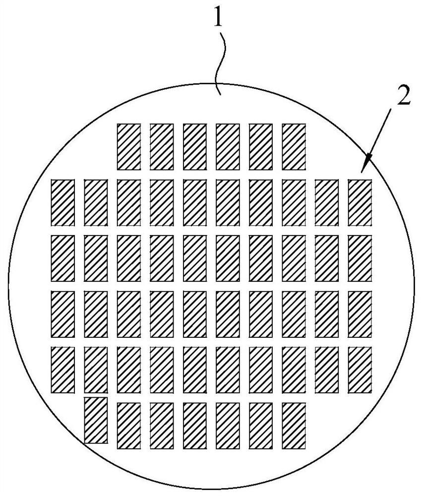
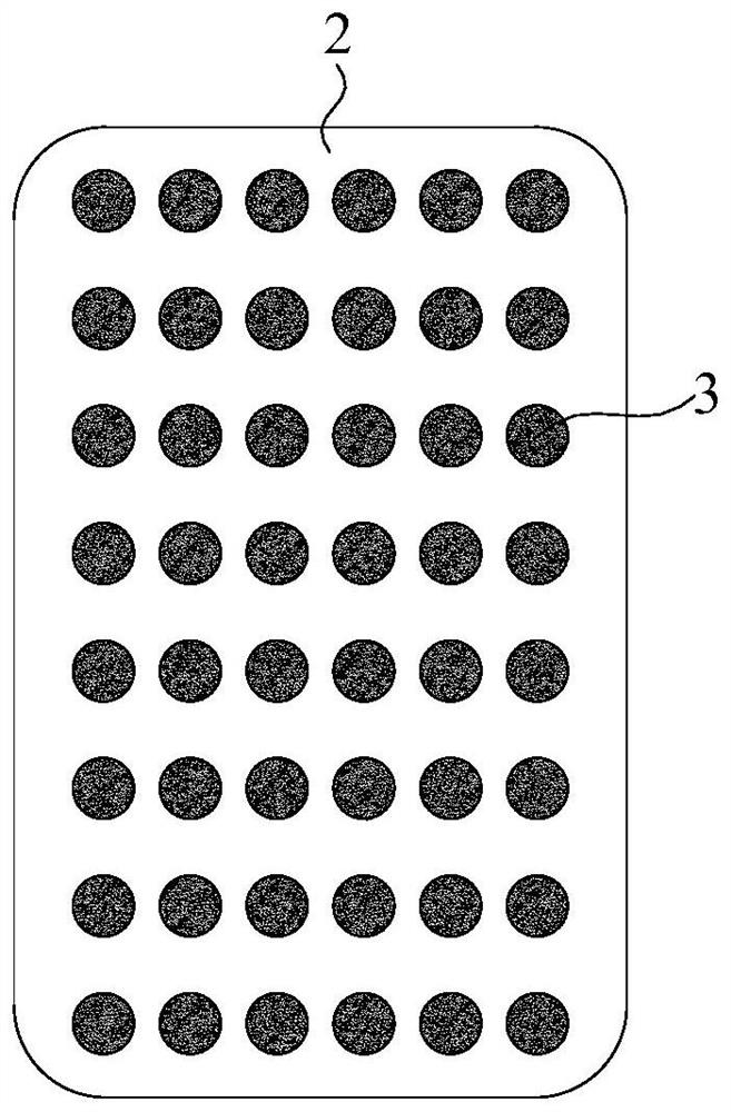
[0032] In order to describe the technical content, structural features, achieved goals and effects of the invention in detail, the following will be described in detail in conjunction with the embodiments and accompanying drawings, wherein the positional relationship of "upper" and "lower" described in this specification is respectively related to that of the appended Figure 7 corresponding to the upper and lower.

[0033] In addition, in this application, whenever "below", "below", "below", "below", "above", "on", "below" Spatially relative terms such as "upper", "higher", "side" (eg, as in "side wall"), etc., are used to describe the relationship between one element and another (other) element as shown in the drawings. relative positional relationship. Spatially relative terms are intended to encompass different orientations of the device in use, operation and / or manufacture in addition to the orientation depicted in the figures. For example, if the device in the figures ...


PUM

PropertyMeasurementUnit
Wavelengthaaaaaaaaaa

Abstract

According to the manufacturing method of the micro-display device provided by the invention, the positive or negative three-dimensional structures are prepared on a pair of wafers to be bonded respectively, the two wafers are pre-bonded under the action of alignment and pressure, and the pre-bonding process is carried out at normal temperature, so that the temperature influence is avoided, and even if a pair of heterogeneous wafers is bonded, the yield of the wafers is greatly improved. The metal plug and the metal pad are bonded by using a heating furnace after pre-bonding, and displacement caused by different thermal expansion coefficients is avoided, the sapphire substrate of the LED is peeled off by using laser after pre-bonding, and finally, the metal plug and the metal pad are bonded by using the heating furnace for heating and bonding.

Description

technical field [0001] The invention belongs to the technical field of semiconductor microdisplays, in particular to a method for manufacturing a microdisplay device. Background technique [0002] Micro-Led is the latest generation of display technology. On the road of industrialization and commercialization of Micro-Led, there are still many technical problems that need in-depth research. Among them, the difficulty in the process of combining the Micro-Led light-emitting chip and the driver chip is the main problem hindering its commercialization. Existing technical solutions include Stamp mass transfer, laser transfer, electrostatic transfer, electromagnetic transfer, fluid self-assembly, etc. However, the above-mentioned technical solutions all have the problems of low single-step yield and long time. Small-sized head-mounted AR / VR requires a small display (about ≤0.5 inches), so the wafer-to-wafer solution has the advantages of high yield and short time. However, the ...

Claims


Application Information

Patent Timeline
IPC IPC(8): H01L27/15H01L33/00H01L33/62
Inventor 岳大川
Owner JIHUA LAB
Learn More