Crystal oscillation circuit, integrated circuit, and electronic device

A crystal oscillation and circuit technology, applied in the field of integrated circuits, electronic equipment, and crystal oscillation circuits, can solve the problems of poor oscillation amplitude and power consumption control, high power consumption, etc. Simple structure design

Pending Publication Date: 2022-04-12
HEFEI CHIPSEA ELECTRONICS TECH CO LTD
View PDF0 Cites 0 Cited by
  • Summary
  • Abstract
  • Description
  • Claims
  • Application Information

AI Technical Summary

Problems solved by technology

[0003] In different integrated circuit processes, the current of the crystal oscillator circuit is also different, and the energy loss of the quartz crystal at the same resonant frequency is also different. In order for the crystal oscillator to work normally, the current must meet the worst working conditions of the crystal oscillator circuit, but When the working condition of the current is too bad, it will cause a lot of power consumption. An existing crystal oscillator circuit controls the oscillation amplitude and power consumption of the crystal oscillator by detecting the peak value of the oscillation amplitude of the crystal oscillator circuit. In the crystal oscillator of the background technology In the oscillation circuit, when the wide voltage range is different or the process of the integrated circuit is different, the control effect of the oscillation amplitude and power consumption is not good.

Method used


Image

  • Crystal oscillation circuit, integrated circuit, and electronic device
  • Crystal oscillation circuit, integrated circuit, and electronic device
  • Crystal oscillation circuit, integrated circuit, and electronic device

Examples


Embodiment Construction

[0050] The technical solutions in the embodiments of the present invention will be clearly and completely described below in conjunction with the drawings in the embodiments of the present invention. It should be clear that the described embodiments are only some of the embodiments of the present invention, not all of them. Based on the embodiments of the present invention, all other embodiments obtained by persons of ordinary skill in the art without making creative efforts belong to the protection scope of the present invention.

[0051] It should be noted that in the description of the embodiment, the suffixes of "module" and "unit" are used to facilitate the description of the application, and they have no specific meaning in themselves; and the "connection" described in the embodiment is all Refers to an electrical connection, which can be a direct connection or an indirect connection.

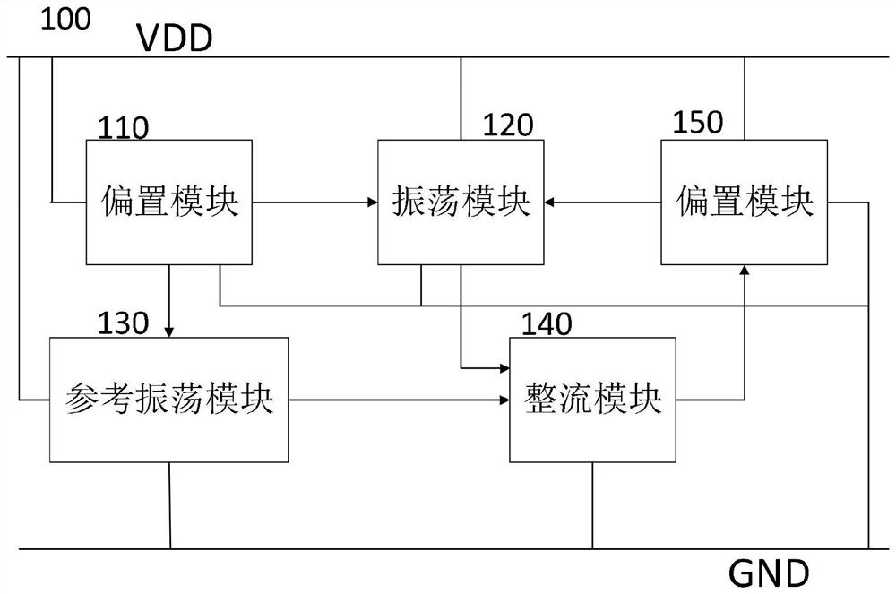
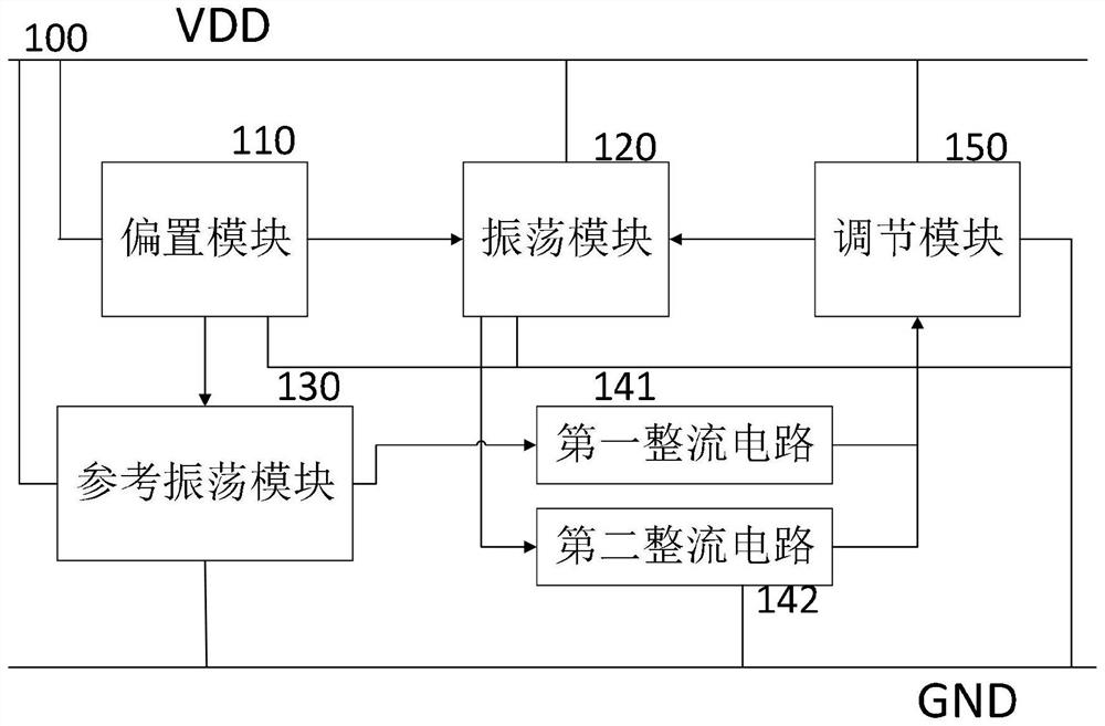
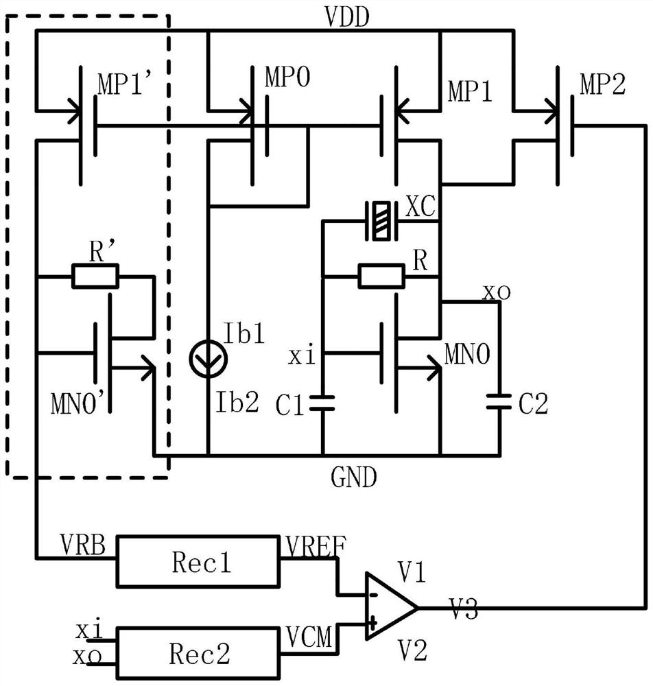
[0052]Embodiments of the present application provide a crystal oscillation circuit, ...


PUM


Abstract

The invention discloses a crystal oscillation circuit, an integrated circuit and electronic equipment, and the circuit comprises an oscillation module which is used for generating a first oscillation signal and a second oscillation signal, and outputting the first oscillation signal and the second oscillation signal to a rectification module; the reference oscillation module is used for generating a reference common-mode signal and outputting the reference common-mode signal to the rectification module; the rectification module is used for respectively generating a reference voltage signal and a rectification signal according to the reference common-mode signal and the oscillation signal and outputting the reference voltage signal and the rectification signal to the adjusting module; the adjusting module is used for generating an adjusting voltage signal according to the reference voltage signal and the rectification signal to control the adjusting current and outputting the adjusting current to the oscillation module to control the amplitudes of the first oscillation signal and the second oscillation signal; and the bias module is used for providing working conditions for the oscillation module and the reference oscillation module. The power consumption of the oscillation process of the crystal oscillation circuit is reduced, the circuit area is reduced, and the oscillation amplitude of the crystal oscillation circuit is accurately controlled when the wide voltage and the integrated circuit process change.

Description

technical field [0001] The invention relates to the technical field of electronic circuits, in particular to a crystal oscillation circuit, an integrated circuit and electronic equipment. Background technique [0002] In ultra-high-precision integrated circuit products such as RTC timing, Gigabit Ethernet communication and other products, the clock generated by the RC oscillator circuit has been difficult to meet the application requirements of these products. In order to meet the application requirements, crystal oscillator circuits are usually used to generate frequencies For a stable clock, the crystal oscillation circuit is composed of an off-chip quartz crystal and an on-chip integrated circuit. The quartz crystal is a passive component that will generate energy loss during the oscillation process. Therefore, the circuit needs to provide energy to maintain the oscillation state of the quartz crystal. [0003] In different integrated circuit processes, the current of the...

Claims


Application Information

Patent Timeline
IPC IPC(8): H03B5/32
CPCH03B5/32
Inventor 刘帅锋
Owner HEFEI CHIPSEA ELECTRONICS TECH CO LTD
Why Eureka
Try Eureka