
A modular high-speed electrical impedance imaging device and method of use

An electrical impedance imaging and modular technology, applied in the fields of application, material resistance, medical science, etc., can solve the problems of increasing cost, reducing system performance, affecting system performance, etc., achieving high-speed detection capability and simplifying control connections.

Active Publication Date: 2022-08-09
HANGZHOU UTRON TECH CO LTD
View PDF6 Cites 0 Cited by
  • Summary
  • Abstract
  • Description
  • Claims
  • Application Information

AI Technical Summary

Problems solved by technology

[0008] 1. The electrodes are connected to the A / D through a multi-way switch, which is not conducive to the design transfer of different electrode quantity systems;
[0009] 2. The structure of the connection is complicated, resulting in complicated control design and increased cost;
[0010] 3. The switching switch of the number of electrodes affects the system performance as a whole;
[0011] 4. The design of system self-test reduces system performance

Method used


Image

  • A modular high-speed electrical impedance imaging device and method of use
  • A modular high-speed electrical impedance imaging device and method of use
  • A modular high-speed electrical impedance imaging device and method of use

Examples


Embodiment 2

[0071] The connection modes of the ports added in Embodiment 2 are as follows:

[0072] About the line of the VL port: the output port VL of the MCU is connected with the input port VL of the independent electrode module N, the output port VL of the independent electrode module N is connected with the input port VL of the independent electrode module N-1, until the output of the independent electrode module 2 The port VL is connected with the input port VL of the independent electrode module 1, and the output port VL of the independent electrode module 1 does not need to be connected;

[0073] Regarding this line of CON: the output port CON of the MCU is connected to the input port CON of the independent electrode module N, the output port CON of the independent electrode module N is connected to the input port CON of the independent electrode module N-1, until the The output port CON is connected to the input port CON of the independent electrode module 1, and the output port...


PUM


Abstract

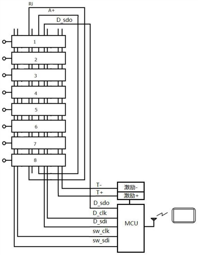
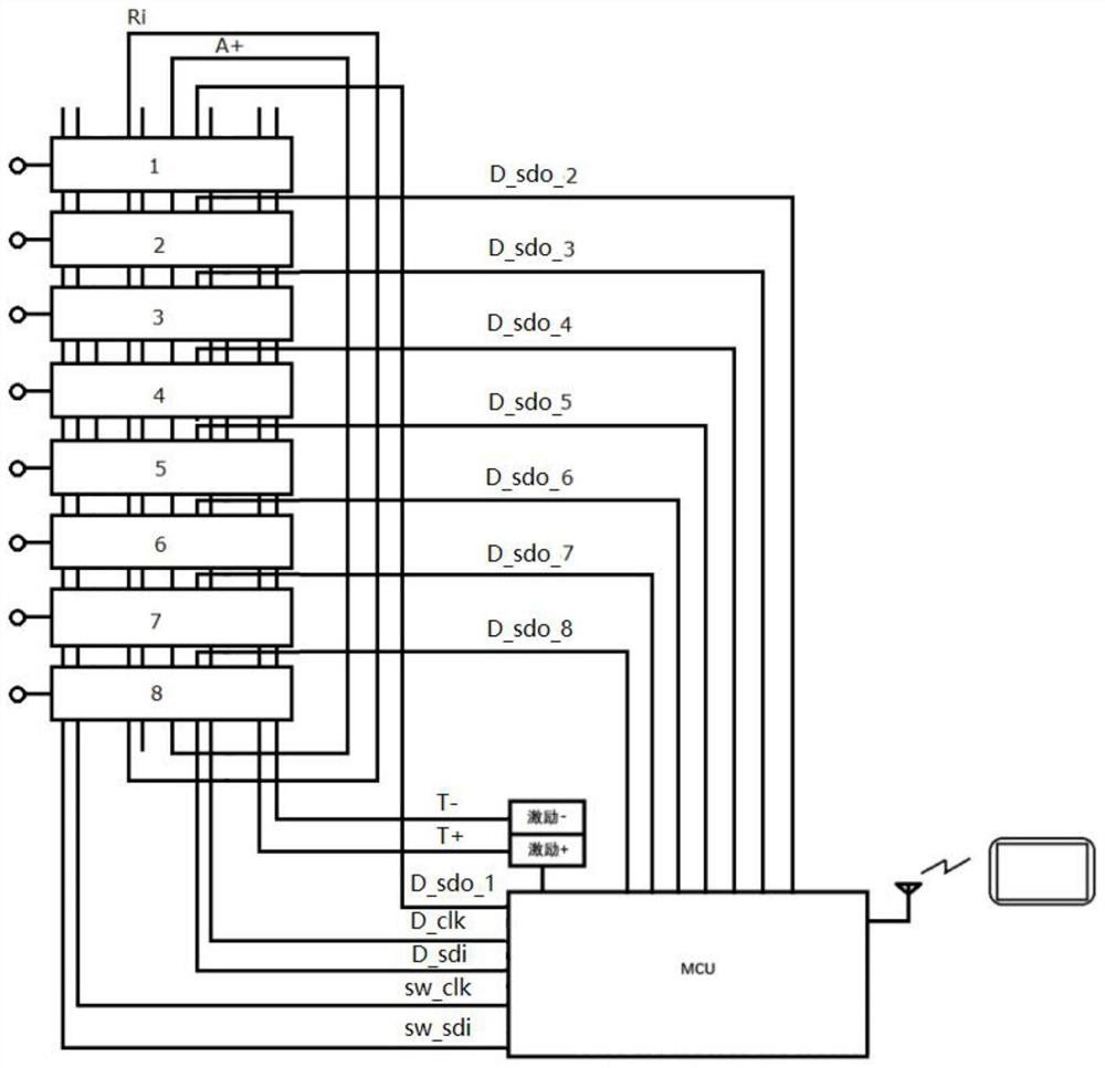
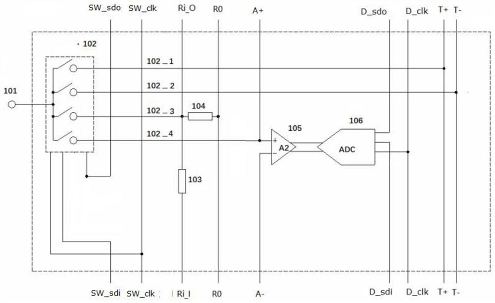
The invention discloses a modular high-speed electrical impedance imaging device and a method for using the same. The device comprises N independent electrode modules, an MCU connected to the independent electrode modules, positive excitation and negative excitation connected to the MCU, and N independent electrode modules. Including independent electrode module 1, independent electrode module 2 to independent electrode module N, independent electrode module includes input port and output port, each independent electrode module is connected with output port through input port, MCU is connected with input port of independent electrode module , each independent electrode module is connected to an electrode. The present invention implements systems with different numbers of electrodes according to a unified design scheme by means of a system bus. This modular design method allows the system to be used in the usual 8, 16, and 32 systems without changing the system structure, and can even be directly used in more electrode systems to achieve three-dimensional multi-slice applications.

Description

technical field [0001] The invention belongs to the field of electrical impedance imaging, in particular to a modularized high-speed electrical impedance imaging device and a method of using the same. Background technique [0002] The electrical impedance imaging device is a multi-electrode control system, and the low-speed electrical impedance imaging device basically consists of 4 multiplex switches. High-speed electrical impedance imaging devices require simultaneous acquisition, so each electrode requires electrode amplification and digital-to-analog conversion detection processing, which makes the system much more complicated than low-speed devices. This brings about the problem that different numbers of electrodes used for different purposes require different system designs. [0003] Chinese patent CN2010800394959 Electrical Impedance Imaging discloses an apparatus for electrical impedance imaging comprising electrodes arranged on an electrode carrier in an arrangemen...

Claims


Application Information

Patent Timeline
Patent Type & Authority Patents(China)
IPC IPC(8): A61B5/0536G01N27/04
CPCA61B5/0536G01N27/04
Inventor 石崇源尤富生宣和均
Owner HANGZHOU UTRON TECH CO LTD
Learn More