Light detection device

A photodetection device and photodetector technology, which is applied in measurement devices, photometry, optical radiation measurement, etc., can solve problems such as complicated process steps, and achieve the effects of reducing the number, shortening the frequency sweeping time, and reducing the pixel area.

Pending Publication Date: 2022-04-22
AU OPTRONICS CORP
View PDF5 Cites 0 Cited by
  • Summary
  • Abstract
  • Description
  • Claims
  • Application Information

AI Technical Summary

Problems solved by technology

Furthermore, since the photodetector needs to align the color resistance for the corresponding light band, it also complicates the process.

Method used


Image

  • Light detection device
  • Light detection device
  • Light detection device

Examples


Embodiment Construction

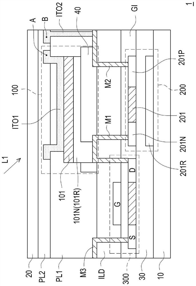
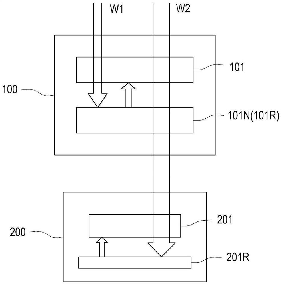
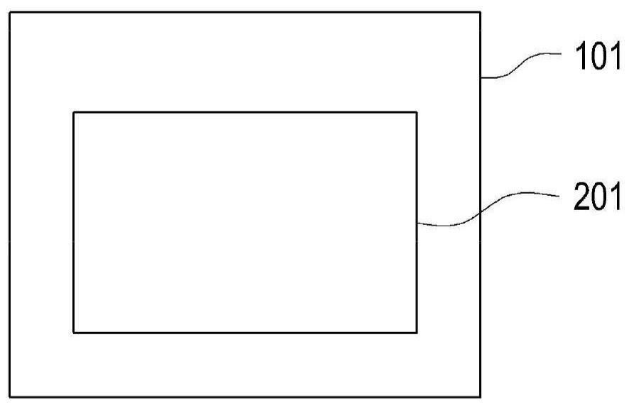
[0038] refer to figure 1 , which shows a schematic cross-sectional view of a photodetector according to an embodiment of the present invention. The photodetection device 1 includes a substrate 10 , a protective layer 20 , a first photodetector 100 , a second photodetector 200 , and a switching element 300 . The first photodetector 100 is disposed on the substrate 10 and includes a first active layer 101 . The second photodetector 200 is disposed between the substrate 10 and the first photodetector 100 , and the second photodetector 200 includes a second active layer 201 . The switch element 300 is a thin film transistor and is disposed on the substrate 10 , and is disposed on the same layer as the second photodetector 200 to shorten the process steps. The horizontal projection of the second active layer 201 on the substrate 10 completely falls within the horizontal projection of the first active layer 101 on the substrate 10, and the negative electrode 101N of the first phot...


PUM

PropertyMeasurementUnit
thicknessaaaaaaaaaa
thicknessaaaaaaaaaa
thicknessaaaaaaaaaa

Abstract

A light detection device includes a substrate, a first light detector, a second light detector, and a switching element. The first photodetector is disposed on the substrate and includes a first active layer. The second photodetector is disposed between the substrate and the first photodetector, and the second photodetector includes a second active layer. The switch element is arranged on the substrate. The horizontal projection of the second active layer on the substrate completely falls within the horizontal projection of the first active layer on the substrate, and the negative electrode of the first light detector and the negative electrode of the second light detector are electrically connected with the switch element through the first metal layer.

Description

technical field [0001] The invention relates to a light detection device. Background technique [0002] Photodetection devices detect the presence of light using the process of generating electrical signals from electromagnetic waves (light). However, in conventional photodetection devices, photodetectors corresponding to different light bands are often arranged in the same layer, resulting in a large overall pixel area. Moreover, since the photodetectors corresponding to different light bands usually use different switching elements to control the frequency scanning, the aperture ratio of the photodetector device is small. Under the above architecture, there is a time difference between frequency sweeps of different optical bands, and the overall frequency sweep time is long. Furthermore, since the photodetector needs to align the color resist for the corresponding light band, the process is also complicated. Contents of the invention [0003] The object of the present...

Claims


Application Information

Patent Timeline
Patent Type & Authority Applications(China)
IPC IPC(8): G01J1/04G01J1/44
CPCG01J1/0407G01J1/44H01L31/0224G01J1/4228G01J1/0209G01J1/0488H01L31/02327G01J3/28
Inventor 黄彦棠
Owner AU OPTRONICS CORP
Why Eureka
Try Eureka