PCB defect detection and identification method based on MAIRNet

A defect detection and recognition method technology, applied in the field of machine vision and deep learning, to achieve the effect of easy operation, good detection and recognition effect, and less manual assistance.

Pending Publication Date: 2022-05-03
NANJING NORMAL UNIVERSITY
View PDF0 Cites 1 Cited by
  • Summary
  • Abstract
  • Description
  • Claims
  • Application Information

AI Technical Summary

Problems solved by technology

[0006] Purpose of the invention: In order to overcome the deficiencies in the existing technology, provide a PCB defect detection and identification method based on MAIRNet, using the detection method based on deep learning and machine vision to replace the traditional detection method, the cost is relatively low in actual application scenarios, There is no need for an expensive automatic optical inspection (AOI) system, and at the same time, compared with manual inspection and contact inspection, the efficiency is greatly improved, and it is not easy to cause damage to PCB surface components, and the method provided by the invention is based on a neural network model. The complexity is low, and it is easy to be transplanted to the embedded development board and applied to the actual industrial production inspection. At the same time, it can realize the detection function of multiple types of defect targets in a single inspection operation, improve the efficiency and reliability of production, and meet the requirements of high performance. , the production demand of high-complexity products can greatly improve the overall detection level of PCB on the production line of smart grid equipment boards, and has important practical application value

Method used


Image

  • PCB defect detection and identification method based on MAIRNet
  • PCB defect detection and identification method based on MAIRNet
  • PCB defect detection and identification method based on MAIRNet

Examples


Embodiment Construction

[0062] Below in conjunction with accompanying drawing and specific embodiment, further illustrate the present invention, should be understood that these embodiments are only for illustrating the present invention and are not intended to limit the scope of the present invention, after having read the present invention, those skilled in the art will understand various aspects of the present invention Modifications in equivalent forms all fall within the scope defined by the appended claims of this application.

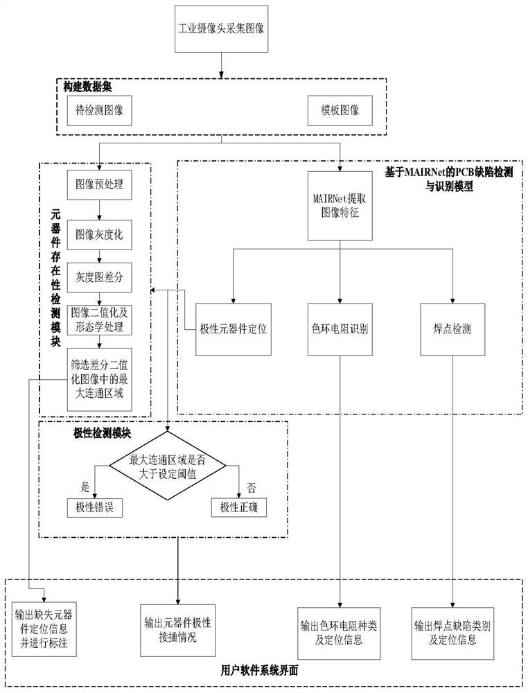
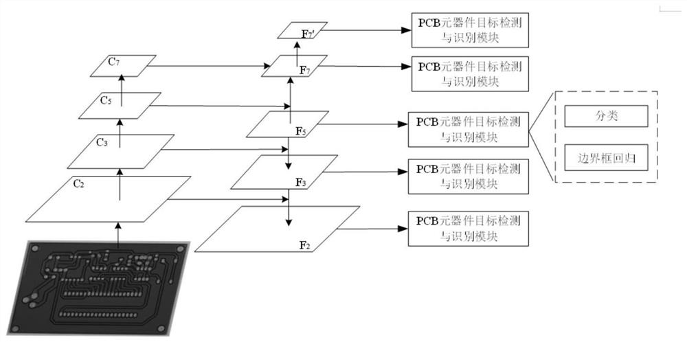
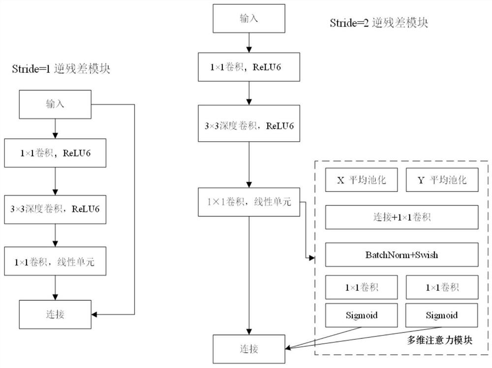
[0063] The invention provides a PCB defect detection and identification method based on multidimensional attention enhancement neural network (MAIRNet), such as figure 1 As shown, it includes the following steps:

[0064] S1: Collect the images to be inspected and the template images on both sides of the PCB. Among them, the images to be inspected have missing components, wrong polarity of components, wrong connection of color ring resistors, and solder joint defects. D...


PUM


Abstract

The invention discloses a PCB defect detection and identification method based on MAIRNet, and the method comprises the steps: collecting a PCB template image and a to-be-detected image, constructing a data set, and dividing the data set into a test set image and a training set image; detecting whether a component is missing or not, and finally outputting missing component positioning information and marking the missing component positioning information in the to-be-detected image; outputting the positioning condition of the polar component, the color ring resistor type and positioning information and the welding spot defect type and positioning information; outputting the cut PCB polarity component to-be-detected image and the template image, constructing a PCB component polarity discrimination method, and outputting the polarity plugging condition of the component; and summarizing and displaying the acquired information. The method can detect and identify common problems of component missing, component polarity plugging errors, welding spot defects and the like on the surface of the PCB, outputs position information and category information of a defect area, can detect and identify the category of the color ring resistor, and has remarkable advantages compared with a manual detection mode.

Description

technical field [0001] The invention relates to the technical field of machine vision and deep learning, in particular to a method for detecting and identifying PCB defects based on MAIRNet. Background technique [0002] With the rapid development of machine vision and artificial intelligence technology, deep learning, neural network and other technologies are gradually applied to the process of industrial inspection. PCB has the characteristics of high density, light weight, and high integration, which also makes the PCB defect detection process face the problems of diversification of target components, small size of detection objects, and difficulty in identification. [0003] The current main methods of PCB inspection are mainly divided into three categories: manual visual inspection, contact inspection and non-contact inspection. Manual visual inspection has the problem of inefficiency, and contact inspection can easily damage PCB surface components. With the developmen...

Claims


Application Information

Patent Timeline
Patent Type & Authority Applications(China)
IPC IPC(8): G06T7/00G06T7/33G06T5/00G06T5/30G06N3/04G06N3/08
CPCG06T7/0004G06T7/33G06T5/002G06T5/007G06T5/30G06N3/08G06T2207/20036G06T2207/20081G06T2207/20084G06T2207/30141G06N3/048G06N3/045
Inventor 谢非章悦张瑞杨嘉乐夏光圣吴佳豪郑鹏飞张培彪王慧敏
Owner NANJING NORMAL UNIVERSITY
Why Eureka
Try Eureka