Process control method and system based on X-ray detection

A detection system, X-ray technology, applied in the field of process control, can solve the problems of lack of resolution and imaging speed of X-ray system, slow integrated circuit detection, etc.

Pending Publication Date: 2022-05-06
BRUKER NANO INC
View PDF1 Cites 0 Cited by
  • Summary
  • Abstract
  • Description
  • Claims
  • Application Information

AI Technical Summary

Problems solved by technology

[0003] However, existing X-ray systems lack sufficient resolution and imaging speed to meet the needs of high-resolution, high-throughput IC and electronic package inspection
For example, traditional computed tomography (CT) using X-rays may take multiple X-ray image slices of the inspected object and use a large number of slices to build a 3D model of the object, so it is very slow and unsuitable for IC inspection

Method used


Image

  • Process control method and system based on X-ray detection
  • Process control method and system based on X-ray detection
  • Process control method and system based on X-ray detection

Examples


Embodiment Construction

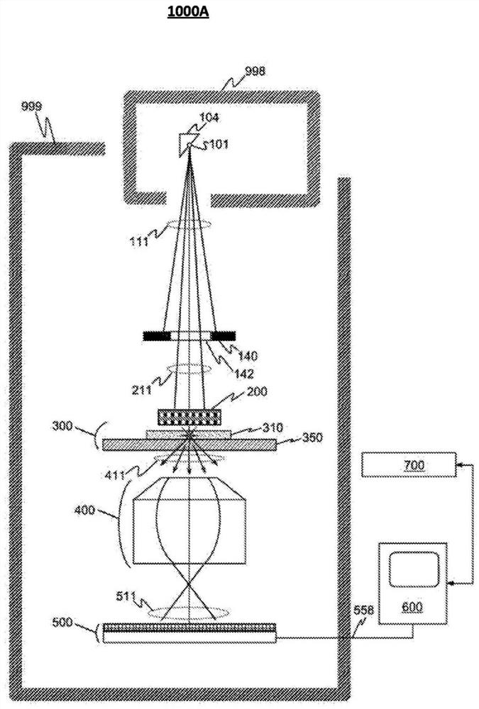
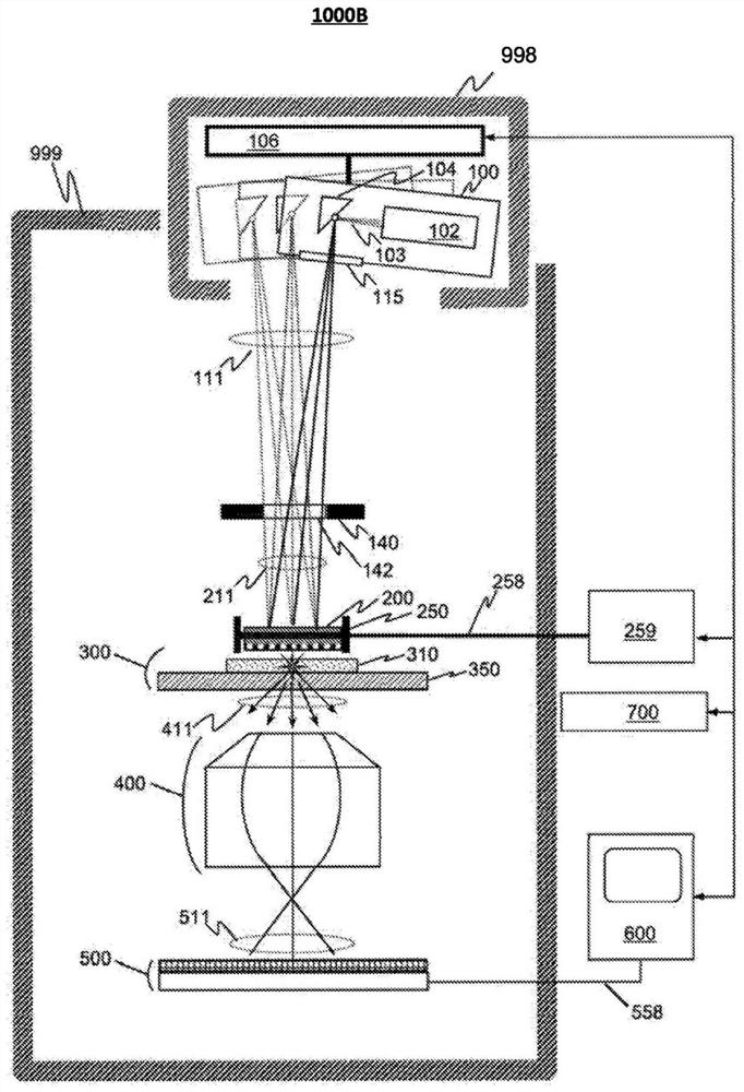
[0014] Automatic high-speed X-ray inspection system

[0015] X-ray system frame

[0016] The systems and methods disclosed herein relate to a system or use of a system that illuminates an object to be inspected or inspected with X-rays that convert the X-rays into visible (or near-visible) photons, forming visible (or near-visible) photons images, and then convert the images into electronic form. Accordingly, various embodiments of the X-ray imaging system will be described first, followed by various embodiments of methods and systems utilizing the X-ray imaging system.

[0017] Although a wide variety of objects may be inspected or inspected using the apparatus disclosed herein, it is contemplated that it is particularly applicable to the inspection and inspection of integrated circuit wafer and package assemblies. One example of this is a silicon interposer, including silicon with multiple TSVs, but the invention can also be used to inspect integrated circuits (ICs) th...


PUM

PropertyMeasurementUnit
divergenceaaaaaaaaaa
quantum efficiencyaaaaaaaaaa
refractive indexaaaaaaaaaa

Abstract

In an embodiment, an X-ray detection system may capture one or more X-ray images for a sample of interest processed by a first tool. The X-ray detection system may be online with the first tool, and its detection speed may be 300 mm2 or more per minute. The system may determine, in real time, metrology information related to the sample of interest based on the X-ray image. The metrology information may indicate that a sample parameter associated with the sample of interest exceeds a predetermined range. The system may provide instructions or data to one or more first tools or one or more second tools to adjust process parameters associated with the respective tools according to the metrology information. The adjusted process parameters may reduce the probability of error in processing respective tools for processing subsequent samples related to sample parameters beyond a predetermined range.

Description

technical field [0001] The invention relates to process control based on X-ray inspection results. Background technique [0002] Integrated circuits can be fabricated to include 3D or 2.5D structures. Since the optical photons or electrons used to inspect silicon wafers cannot penetrate ICs, interposers, or Cu-Cu dies for die bonding to provide an adequate view of the interior of packaged ICs, optical Inspection techniques that photonically or electronically inspect silicon wafers cannot be used to inspect 3D and 2.5D IC packages. Optical inspection methods also cannot inspect or metrology partially encapsulated components, a key requirement for process control. Since X-rays can penetrate multilayer packages, X-ray inspection can provide an internal view of assembled devices. [0003] However, existing X-ray systems lack sufficient resolution and imaging speed to meet the needs of high-resolution, high-throughput IC and electronic package inspection. For example, traditi...

Claims


Application Information

Patent Timeline
Patent Type & Authority Applications(China)
IPC IPC(8): G01N23/04
CPCG01N23/04G01T1/20G06T7/001G06T2207/20081G06T2207/10116G06T2207/10016G06T2207/30141G06T2207/30148G06T2207/30152G01N2223/401G01N2223/6466G01N2223/505G06N20/20G06V2201/06G06V10/82G06N5/01G06N3/045G06F18/214G06F18/24G01N23/043G01N23/083G01N23/18G06T5/007G06F30/398G06N20/00H05K1/115H05K3/4038H01L21/67288G01N2223/04G01N2223/426G06T2207/10081G06T2207/20024G06T2207/20208G06T2207/30004G06F2115/12G06F2119/18G06T7/0014G06T7/0012
Inventor 大卫·刘易斯·阿德勒斯科特·约瑟夫·朱勒
Owner BRUKER NANO INC
Why Eureka
Try Eureka