
Low-cost and high-bandwidth packaging substrate structure and optical module

A packaging substrate, high-bandwidth technology, applied in the field of optical communication, can solve the problems of high cost and high power consumption, and achieve the effects of simple structure, high bandwidth and cost reduction

Pending Publication Date: 2022-05-10
成都新易盛通信技术股份有限公司 +1
View PDF0 Cites 0 Cited by
  • Summary
  • Abstract
  • Description
  • Claims
  • Application Information

AI Technical Summary

Problems solved by technology

In addition, because the laser needs to work within a certain temperature range to ensure optimal performance, the current 400G and 800G products mostly use TEC (ThermoElectric Cooler) to control the temperature, but this solution has the problems of high cost and high power consumption

Method used


Image

  • Low-cost and high-bandwidth packaging substrate structure and optical module
  • Low-cost and high-bandwidth packaging substrate structure and optical module
  • Low-cost and high-bandwidth packaging substrate structure and optical module

Examples


Embodiment Construction

[0020] The technical solutions in the embodiments of the present invention will be described below with reference to the drawings in the embodiments of the present invention.

[0021] It should be noted that like numerals and letters denote similar items in the following figures, therefore, once an item is defined in one figure, it does not require further definition and explanation in subsequent figures. Meanwhile, in the description of the present invention, the terms "first", "second", etc. are only used to distinguish descriptions, and cannot be understood as indicating or implying relative importance.

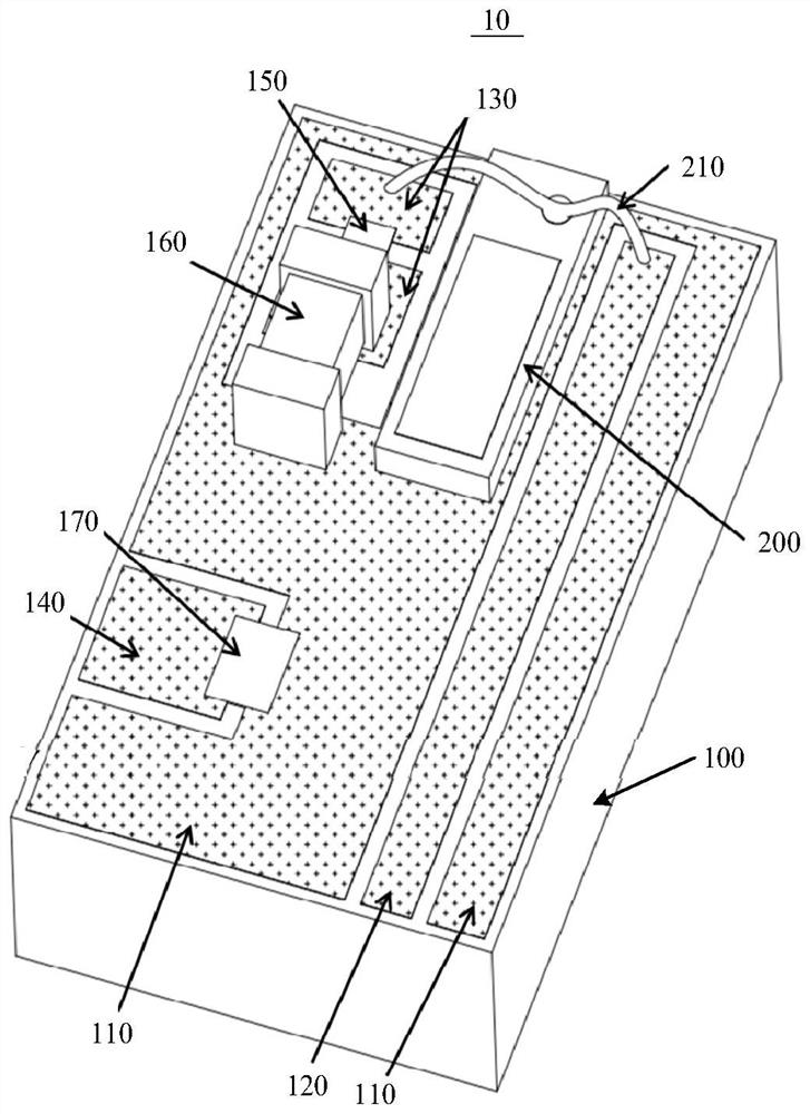
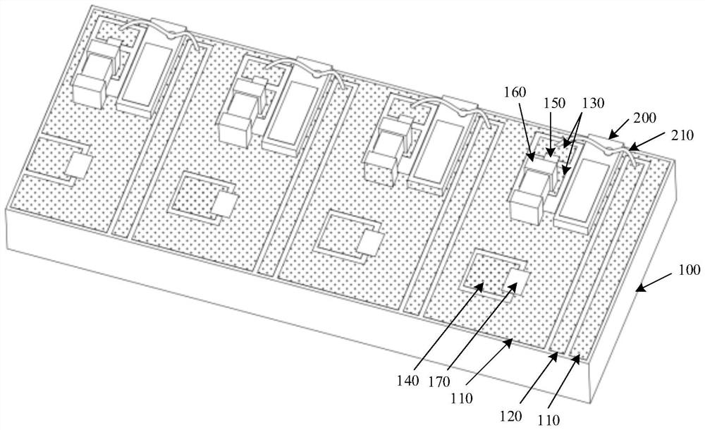
[0022] Please see figure 1 and figure 2 , figure 1 A schematic diagram of the first packaging substrate structure provided by the embodiment of the present invention; figure 2 It is a schematic diagram of the first packaging substrate structure provided by the embodiment of the present invention.

[0023] The embodiment of the present invention provides a low-cost an...


PUM


Abstract

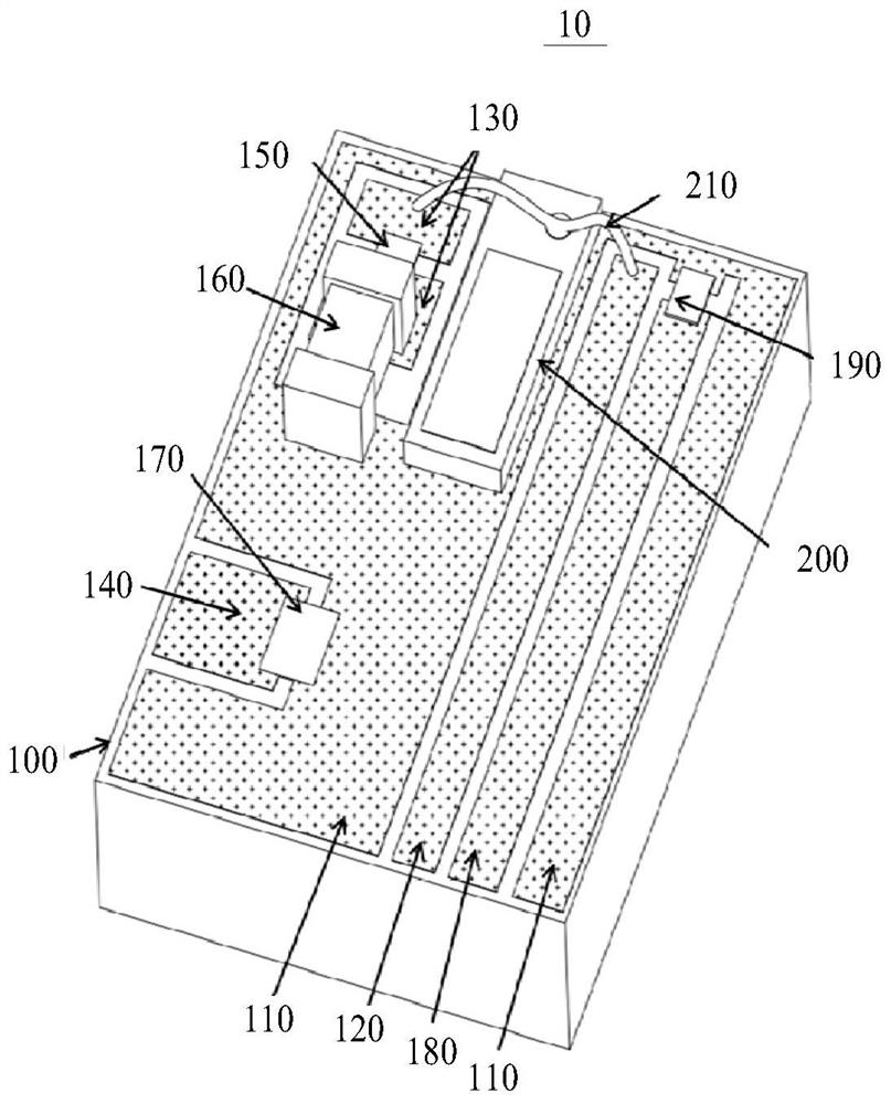
The invention provides a low-cost and high-bandwidth packaging substrate structure and an optical module. The low-cost and high-bandwidth packaging substrate structure comprises a substrate; the circuit structures are arranged on the substrate in parallel; the circuit structure comprises a grounding layer, a first signal line layer, a high-frequency impedance matching circuit and a heating circuit which are arranged on a substrate, the grounding layer separates the first signal line layer, the high-frequency impedance matching circuit and the heating circuit, and gaps exist between the layers. A laser close to the edge of the substrate is mounted on the grounding layer; the high-frequency impedance matching circuit and the first signal line layer are oppositely arranged on the two sides of the laser; the heating circuit is arranged on the lower sides of the high-frequency impedance matching circuit and the laser; the high-frequency impedance matching circuit comprises a first metal layer and a second metal layer which are arranged at an interval; a first resistor is bridged between the first metal layer and the second metal layer; a filter capacitor is bridged between the second metal layer and the grounding layer; the first metal layer, the first signal line layer and the upper surface of the laser are connected through arranged gold threads.

Description

technical field [0001] The invention relates to the technical field of optical communication, in particular to a low-cost and high-bandwidth packaging substrate structure and an optical module. Background technique [0002] At present, with the rapid development of emerging applications such as autonomous driving, data centers, and metaverses, single-channel transmission rates are gradually increasing, single-channel 25G Baud and 50G Baud have been gradually applied in batches, and higher-speed lasers are gradually being used in the industry chain. roll out. Generally, the laser in the optical device or optical module is connected to the PCB board by means of the substrate or ceramic housing below it. The higher bandwidth of the packaging substrate structure is more conducive to improving its overall performance. In addition, since the laser needs to work within a certain temperature range to ensure optimal performance, the current 400G and 800G products mostly use TEC (Th...

Claims


Application Information

Patent Timeline
Patent Type & Authority Applications(China)
IPC IPC(8): H01S5/02315H01S5/0239H01S5/02345H01S5/024
CPCH01S5/02315H01S5/0239H01S5/02345H01S5/02453
Inventor 黄晓雷武锐罗智仲柳
Owner 成都新易盛通信技术股份有限公司
Features
  • Generate Ideas
  • Intellectual Property
  • Life Sciences
  • Materials
  • Tech Scout
  • Unparalleled Data Quality
  • Higher Quality Content
  • 60% Fewer Hallucinations
Learn More