
Bare chip taking-out method

A bare chip and sample technology, applied in the field of bare chip removal, can solve the problems of circuit board corrosion, inability to detect electrical properties, large surface height difference steps, etc., to achieve the effect of keeping the electrical properties unchanged

Pending Publication Date: 2022-05-13
CHANGXIN MEMORY TECH INC
View PDF0 Cites 0 Cited by
  • Summary
  • Abstract
  • Description
  • Claims
  • Application Information

AI Technical Summary

Problems solved by technology

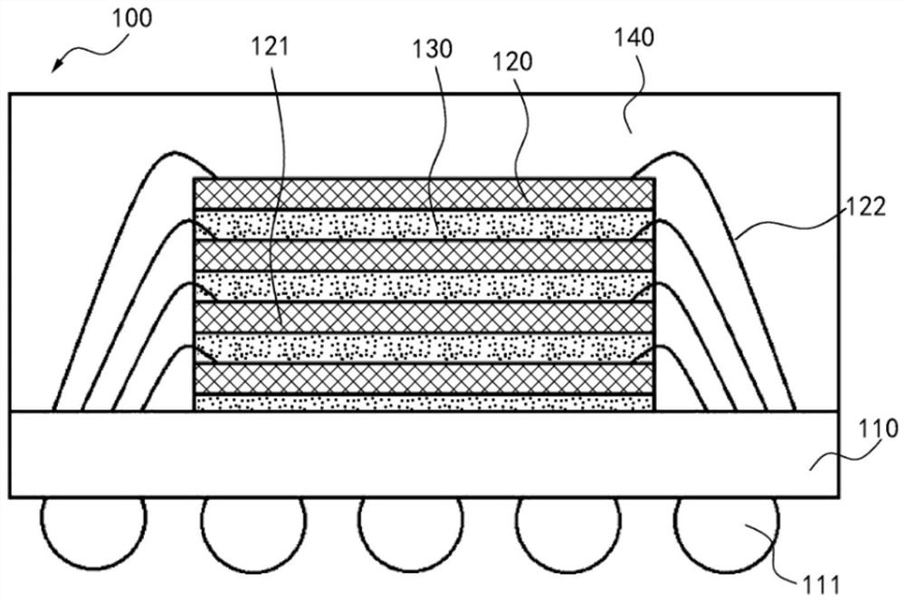
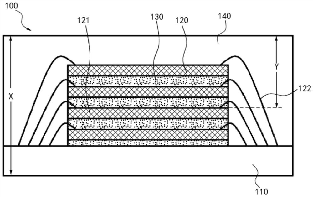
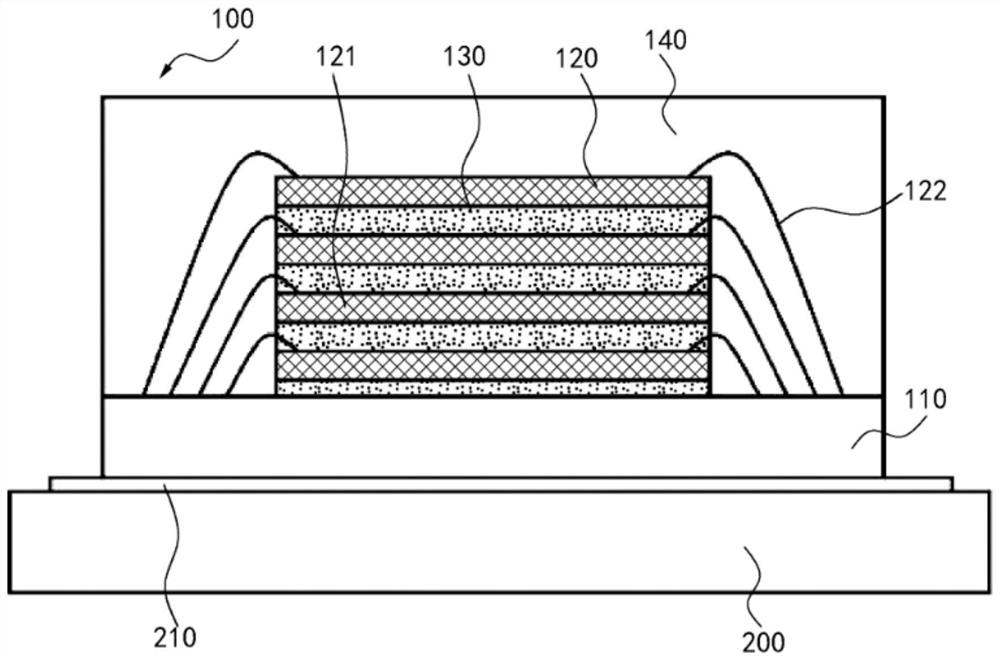
Among them, the existing die removal method is to use high-temperature fuming nitric acid for a long time (more than 1h) to separate the multi-layered die. Since the thickness of the stacked die is ultra-thin (about 50 μm), it will cause the die to be broken. Cracks and circuit board corrosion, resulting in the inability to detect electrical
In order to alleviate the above problems, although the grinding method can be used to grind down to the target die on the lower layer to reduce the soaking time, however, the traditional hand-held grinding disc still has the problem of a large level difference (about 30 μm or more) on the surface of the sample

Method used


Image

  • Bare chip taking-out method
  • Bare chip taking-out method
  • Bare chip taking-out method

Examples


Embodiment Construction

[0065] Typical embodiments embodying the features and advantages of the present invention will be described in detail in the following description. It should be understood that the present invention can have various changes in different embodiments without departing from the scope of the present invention, and that the description and drawings therein are illustrative in nature and not intended to limit the present invention. invention.

[0066] In the following description of various exemplary embodiments of the invention, reference is made to the accompanying drawings, which form a part hereof, and in which are shown by way of example different exemplary structures, systems, and embodiments in which aspects of the invention may be implemented and steps. It is to be understood that other specific arrangements of components, structures, exemplary devices, systems and steps may be utilized and structural and functional modifications may be made without departing from the scope...


PUM

PropertyMeasurementUnit
thicknessaaaaaaaaaa
thicknessaaaaaaaaaa

Abstract

The invention provides a bare chip taking-out method. The bare chip taking-out method comprises the following steps that solder balls on the back face of a sample are removed; the back face of the sample is attached to a grinding jig, and the sample is flattened through a flattener; grinding the front surface of the sample, removing the part positioned on the front surface of the target bare chip, and reserving the part of the bonding film positioned on the front surface of the target bare chip and the lead positioned in the part; the front face of the sample is attached to a grinding jig, and the sample is flattened through a flattener; grinding the back surface of the sample, removing the part on the back surface of the target bare chip, and retaining a layer of bonding film on the back surface of the target bare chip; removing the residual bonding film and packaging material of the sample to obtain a target bare chip; and attaching the back surface of the target bare chip to the glass slide to complete the taking-out of the target bare chip.

Description

technical field [0001] The invention relates to the technical field of detection of integrated circuits, in particular to a method for taking out a bare chip. Background technique [0002] In the integrated circuit packaging structure, in order to increase the capacity per unit area, the packaging is usually performed in a stacked manner. At present, in the detection of integrated circuit packaging structures, the location of failure hotspots can only be accurately located for the die on the current layer. When the die stacked on the lower layer fails, the failure point cannot be located. In order to realize the failure location of the lower die, the lower die must be used to solder the integrated circuit die while keeping the original electrical properties unchanged. Chip circuit board) electrical properties, take out the bare chip, and then do failure location. Among them, the existing die removal method is to use high-temperature fuming nitric acid for a long time (more...

Claims


Application Information

Patent Timeline
Patent Type & Authority Applications(China)
IPC IPC(8): H01L21/66
CPCH01L22/14H01L22/00H01L21/02G01R31/26
Inventor 王坤
Owner CHANGXIN MEMORY TECH INC
Learn More