A gan-based LED epitaxial wafer, epitaxial growth method and LED chip

A LED epitaxial wafer, epitaxial growth technology, applied in the direction of semiconductor devices, electrical components, circuits, etc., can solve the problems of LED luminous efficiency decline, difficult growth of P-type GaN layer, etc., to increase the concentration of activated Mg, improve crystal quality, improve Effect of Ga atomic mobility

Active Publication Date: 2022-07-12
JIANGXI ZHAO CHI SEMICON CO LTD
View PDF0 Cites 0 Cited by
  • Summary
  • Abstract
  • Description
  • Claims
  • Application Information

AI Technical Summary

Problems solved by technology

[0005] Based on this, the object of the present invention is to provide a GaN-based LED epitaxial wafer, an epitaxial growth method and an LED chip, aiming at solving the problem that the low-temperature P-type GaN layer is difficult to grow to the bottom along the V-shaped pit in the existing GaN-based LED epitaxial structure , leading to the problem that LED luminous efficiency decreases

Method used


Image

  • A gan-based LED epitaxial wafer, epitaxial growth method and LED chip
  • A gan-based LED epitaxial wafer, epitaxial growth method and LED chip
  • A gan-based LED epitaxial wafer, epitaxial growth method and LED chip

Examples


Embodiment 1

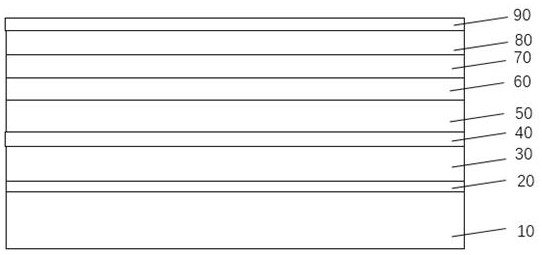
[0031] see figure 1 and figure 2 , shows the GaN-based LED epitaxial wafer in the first embodiment of the present invention, including a substrate 10, a buffer layer 20 stacked in sequence on the substrate 10, an undoped GaN layer 30, an N-type GaN layer 40, a multi-quantum Well layer 50 , low temperature P-type GaN layer 60 , electron blocking layer 70 , P-type GaN layer 80 and P-type contact layer 90 .

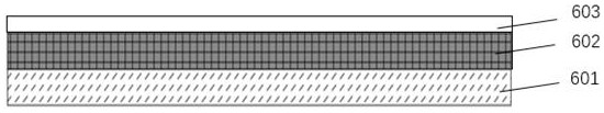
[0032] In this embodiment, the low-temperature P-type GaN layer 60 includes a first low-temperature P-type GaN sub-layer 601, a second low-temperature P-type GaN sub-layer 602, and a third low-temperature P-type GaN sub-layer 603, which are stacked in sequence. Both the low-temperature P-type GaN sublayer 601 and the second low-temperature P-type GaN sub-layer 602 are AlInGaN layers that are heavily doped with Mg, and the third low-temperature P-type GaN sub-layer 603 is a Mg-undoped GaN layer. MOCVD (Metal-organic Chemical Vapor Deposition, referred to as: metal organic ...

Embodiment 2

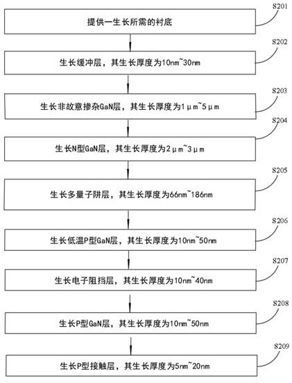
[0037] see image 3 , shows an epitaxial growth method of an LED epitaxial wafer proposed in the second embodiment of the present invention, which is used to prepare the GaN-based LED epitaxial wafer in the above-mentioned first embodiment. The method specifically includes steps S201 to S209, wherein:

[0038] Step S201, providing a substrate required for growth.

[0039] In this embodiment, the substrate is a sapphire substrate, which is an example but not a limitation. In some preferred embodiments of this embodiment, the substrate may also be a silicon substrate, a silicon carbide substrate, a gallium nitride substrate, an oxide Zinc substrates, etc. Among them, the sapphire substrate is selected because of its mature preparation process, large output, low cost, and excellent chemical stability and thermal stability.

[0040] In step S202, a buffer layer is grown, and the growth thickness thereof is 10 nm˜30 nm.

[0041] Specifically, the buffer layer is an AlN layer, whi...

Embodiment 3

[0066] The third embodiment of the present invention provides an LED chip, including the LED epitaxial wafer in the first embodiment. The LED epitaxial wafer can be epitaxially grown by the epitaxial growth method of the LED epitaxial wafer in the second embodiment.

[0067] In this embodiment, the thickness of the low-temperature P-type GaN layer in the LED chip is 20 nm, and the atmosphere is NH when growing the low-temperature P-type GaN layer. 3 / H 2 / N 2 The ratio is 1:1.3:2.3, wherein the thickness of the second low-temperature P-type GaN sub-layer is twice the thickness of the first low-temperature P-type GaN sub-layer, and the thickness of the first low-temperature P-type GaN sub-layer is the same as the thickness of the third low-temperature P-type GaN sub-layer. The layer thicknesses are the same, in addition, the first low temperature P-type GaN sublayer is Al 0.02 In 0.05 Ga 0.93 N layer, second low temperature P-type GaN sublayer is Al 0.007 In 0.05 Ga 0.94...


PUM

PropertyMeasurementUnit
thicknessaaaaaaaaaa
thicknessaaaaaaaaaa
thicknessaaaaaaaaaa

Abstract

The invention provides a GaN-based LED epitaxial wafer, an epitaxial growth method and an LED chip. The GaN-based LED epitaxial wafer includes a first low-temperature P-type GaN sub-layer, a second low-temperature P-type GaN sub-layer and a third low-temperature P-type GaN sub-layer stacked in sequence. The GaN sub-layer, the first low-temperature P-type GaN sub-layer and the second low-temperature P-type GaN sub-layer are all AlInGaN layers heavily doped with Mg, and the third low-temperature P-type GaN sub-layer is a GaN layer, wherein the first low-temperature P-type GaN sub-layer is The concentration of the Al composition in the sublayer is greater than the concentration of the Al composition in the second low temperature P-type GaN sublayer, and the third low temperature P-type GaN sublayer passes through the atmosphere by NH 3 / N 2 / H 2 Fade to NH 3 / N 2 , at the same time, the temperature is gradually increased to grow. The invention can effectively solve the problem that in the existing GaN-based LED epitaxial structure, the low-temperature P-type GaN layer is difficult to grow to the bottom along the V-type pit, which leads to the decrease of the LED luminous efficiency.

Description

technical field [0001] The invention relates to the technical field of LEDs, in particular to a GaN-based LED epitaxial wafer, an epitaxial growth method and an LED chip. Background technique [0002] Light Emitting Diode (LED) is a semiconductor electronic component that can emit light. Due to its small size, high brightness and low energy consumption, it has attracted the attention of more and more researchers. Among them, GaN-based The LED has the advantages of high density, low energy consumption, long life, short response time, no radiation, etc., and is widely used in lighting and display fields. [0003] Among them, there is a phenomenon of quantum efficiency decline in GaN-based LEDs, that is, when the current density is higher, the luminous efficiency of the LED decreases instead. One of the main reasons for this phenomenon is caused by insufficient injection of holes, so how to The issue of improving hole injection efficiency deserves attention. [0004] Traditio...

Claims


Application Information

Patent Timeline
Patent Type & Authority Patents(China)
IPC IPC(8): H01L33/14H01L33/02H01L33/00
CPCH01L33/025H01L33/14H01L33/007
Inventor 程龙郑文杰曾家明高虹胡加辉
Owner JIANGXI ZHAO CHI SEMICON CO LTD
Why Eureka
Try Eureka