
Semiconductor structure, preparation method and application

A semiconductor and gas technology, applied in semiconductor devices, electrical components, circuits, etc., can solve problems such as material electrical properties change, nitride material damage, etc., to reduce heat, reduce contact resistance, and improve application performance.

Pending Publication Date: 2022-05-13
宁波安芯美半导体有限公司
View PDF8 Cites 0 Cited by
  • Summary
  • Abstract
  • Description
  • Claims
  • Application Information

AI Technical Summary

Problems solved by technology

However, plasma etching can cause various forms of damage to nitride materials, resulting in changes in the electrical properties of the material

Method used


Image

  • Semiconductor structure, preparation method and application
  • Semiconductor structure, preparation method and application
  • Semiconductor structure, preparation method and application

Examples


Embodiment Construction

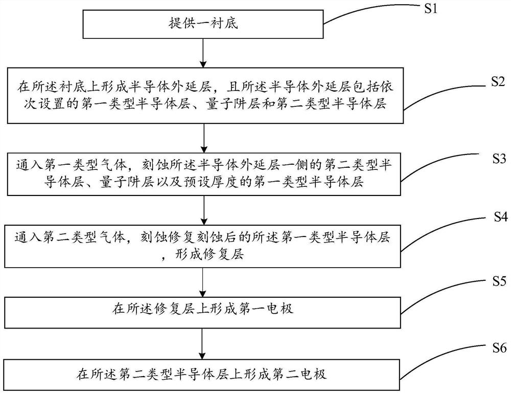
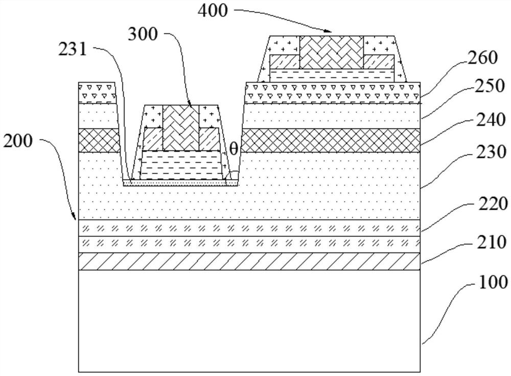
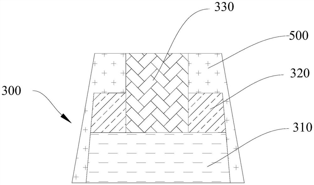
[0039] Embodiments of the present invention are described below through specific examples, and those skilled in the art can easily understand other advantages and effects of the present invention from the content disclosed in this specification. The present invention can also be implemented or applied through other different specific implementation modes, and various modifications or changes can be made to the details in this specification based on different viewpoints and applications without departing from the spirit of the present invention.

[0040] It should be noted that the diagrams provided in this embodiment are only schematically illustrating the basic idea of ​​the present invention, and only the components related to the present invention are shown in the diagrams rather than the number, shape and shape of the components in actual implementation. Dimensional drawing, the type, quantity and proportion of each component can be changed arbitrarily during actual impleme...


PUM

PropertyMeasurementUnit
thicknessaaaaaaaaaa
thicknessaaaaaaaaaa
thicknessaaaaaaaaaa

Abstract

The invention provides a semiconductor structure and a preparation method and application thereof, and the preparation method at least comprises the following steps: providing a substrate; forming a semiconductor epitaxial layer on the substrate, wherein the semiconductor epitaxial layer comprises a first type semiconductor layer, a quantum well layer and a second type semiconductor layer which are arranged in sequence; introducing a first type of gas, and etching the second type of semiconductor layer on one side of the semiconductor epitaxial layer, the quantum well layer and the first type of semiconductor layer with a preset thickness; introducing a second type of gas, and etching and repairing the etched first type of semiconductor layer to form a repairing layer; forming a first electrode on the repairing layer; and forming a second electrode on the second type semiconductor layer. According to the semiconductor structure, the preparation method and the application provided by the invention, the problem of difficulty in ohmic contact of the electrodes of the semiconductor structure can be effectively improved.

Description

technical field [0001] The invention belongs to the field of semiconductor manufacturing, and in particular relates to a semiconductor structure, preparation method and application. Background technique [0002] In recent years, due to the great advantages of high-aluminum component AlGaN-based semiconductor devices in terms of energy saving, environmental protection, and portability, as well as important applications in sterilization and safe communication, especially for the inactivation of new coronaviruses, high-aluminum components Research on AlGaN-based diodes and transistors has attracted much attention. However, AlGaN with high aluminum composition has a larger band gap and higher electron affinity, and it is difficult to achieve high-quality ohmic contacts, which limits the device performance. Furthermore, as the aluminum content in AlGaN increases, the contact problem becomes more difficult due to the lower carrier concentration in the conductive layer. [0003] ...

Claims


Application Information

Patent Timeline
Patent Type & Authority Applications(China)
IPC IPC(8): H01L33/24H01L33/38H01L33/32H01L33/06H01L33/00
CPCH01L33/24H01L33/38H01L33/32H01L33/06H01L33/0075
Inventor 吕振兴齐胜利刘亚柱赵耀张丽
Owner 宁波安芯美半导体有限公司
Learn More