superjunction semiconductor device

A super-junction semiconductor and device technology, applied in the field of super-junction semiconductor devices, can solve the problems of low Miller capacitance Cgd, affecting the withstand voltage level of the device, and fast turn-off speed, so as to increase the Miller capacitance Cgd, improve the EMI problem, The effect of reducing the overshoot voltage

Active Publication Date: 2022-07-15
SEMICON MFG ELECTRONICS (SHAOXING) CORP
View PDF1 Cites 0 Cited by
  • Summary
  • Abstract
  • Description
  • Claims
  • Application Information

AI Technical Summary

Problems solved by technology

In this cellular structure, since the vertically extending P-type doped columns 11 form a shielding effect on the polysilicon gate 14, the Miller capacitance Cgd is relatively low, which easily leads to an excessively fast turn-off speed and a large overshoot voltage, which may can cause serious EMI problems
[0004] Appropriately increasing the Miller capacitance Cgd can reduce the turn-off speed and reduce the overshoot voltage, but blindly increasing the Miller capacitance Cgd will also cause an increase in Qg (gate charge), resulting in greater switching loss, and may also affect the device endurance. Therefore, the preferred way is to increase the Miller capacitance Cgd to reduce the turn-off speed and reduce the overshoot voltage, while avoiding affecting Qg and device withstand voltage performance

Method used


Image

  • superjunction semiconductor device
  • superjunction semiconductor device
  • superjunction semiconductor device

Examples


Embodiment Construction

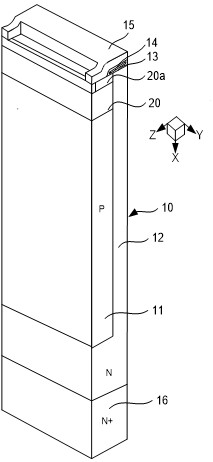
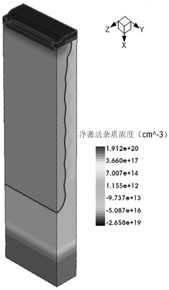
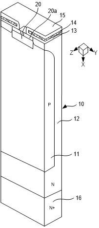
[0030] The superjunction semiconductor device of the present invention will be further described in detail below with reference to the accompanying drawings and specific embodiments. The advantages and features of the present invention will become more apparent from the following description. It should be understood that the drawings in the description are all in a very simplified form and in non-precise scales, and are only used to facilitate and clearly assist the purpose of explaining the embodiments of the present invention. It should be understood that spatially relative terms are intended to encompass different orientations of the device in use or operation in addition to the orientation depicted in the figures. For example, if the structure in the figures is turned over or otherwise oriented in a different manner (eg, rotated), the exemplary term "on" may also include "under" and other orientational relationships.

[0031] It should be noted that, according to differen...


PUM


Abstract

The present invention relates to a superjunction semiconductor device. In at least one cell structure of the superjunction semiconductor device, the first-type body region includes at least two segmented body regions arranged in the third direction, and the source region is disposed in a part of the segmented body region away from the drain region The surface of the gate oxide layer is arranged on the surface of another part of the segmented body region away from the drain region, and the gate is arranged on the surface of the gate oxide layer away from the segmented body region. In this cell structure, The segmented body region where the gate oxide layer and the gate are arranged is separated from the segmented body region where the source region is arranged, which can weaken the shielding effect of the first type doping column on the gate, and can increase the Miller capacitance Cgd compared with the traditional structure. Helps reduce turn-off speed, reduce overshoot voltage, improve EMI problems, and studies have shown that it has less impact on Qg and device withstand voltage performance.

Description

technical field [0001] The present invention relates to the technical field of semiconductors, and in particular, to a superjunction semiconductor device. Background technique [0002] In the superjunction semiconductor device, a longitudinally extending P-type doped column is inserted into the drift region of a traditional power device. In the off state, the PN junction formed by the P-type doped column and the adjacent N-type doped column depletes each other, forming a 3D -RESURF (Reduced Surface Electric Field) effect, a smaller on-resistance Ron can be obtained while meeting the withstand voltage of the device. [0003] like figure 1 and figure 2 As shown, in a cell structure of a superjunction semiconductor device, a P-type body region 20 (P body) is provided on the top of a P-type doping column 11 provided in the drift region 10, and a P-type body region 20 is provided on the top surface of the P-type body region 20 for The N+ source region 20a in contact with the ...

Claims


Application Information

Patent Timeline
Patent Type & Authority Patents(China)
IPC IPC(8): H01L29/06H01L29/08H01L29/423H01L29/78
CPCH01L29/0696H01L29/0847H01L29/42356H01L29/7827
Inventor 苑羽中张玉琦戴银
Owner SEMICON MFG ELECTRONICS (SHAOXING) CORP
Why Eureka
Try Eureka