Integrated circuit chip flatness detection device and method

A testing equipment and integrated circuit technology, applied in the field of integrated circuit chip flatness testing equipment, can solve problems such as low batch testing efficiency, and achieve the effects of avoiding manual cutting, compact structure and high degree of automation

Inactive Publication Date: 2022-05-20
深圳市通恒伟创科技有限公司
View PDF0 Cites 3 Cited by
  • Summary
  • Abstract
  • Description
  • Claims
  • Application Information

AI Technical Summary

Problems solved by technology

[0004] The purpose of the present invention is to solve the problem of low batch detection efficiency in the prior art, and propose a kind of integrated circuit chip flatness detection equipment and method

Method used


Image

  • Integrated circuit chip flatness detection device and method
  • Integrated circuit chip flatness detection device and method
  • Integrated circuit chip flatness detection device and method

Examples


Embodiment Construction

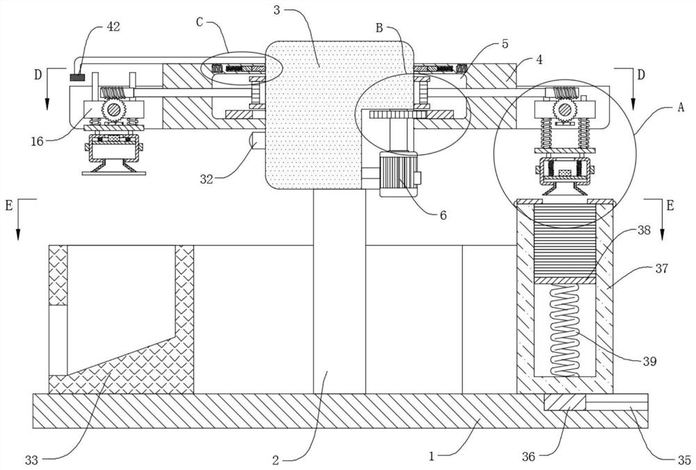
[0039] refer to Figure 1-11 , a kind of integrated circuit chip flatness detection equipment, comprises machine base 1, and the upper surface of machine base 1 is welded with column 2, and column 2 is fixedly connected with fixed block 3, and the side wall of fixed block 3 is fixedly connected with a plurality of detectors 32, as Figure 11 As shown, there are five detectors 32 evenly distributed, one of which detects the bottom surface of the chip, and the remaining four detect the four sides of the chip. Ring, the rotating block 4 is provided with a detection mechanism for flatness detection;

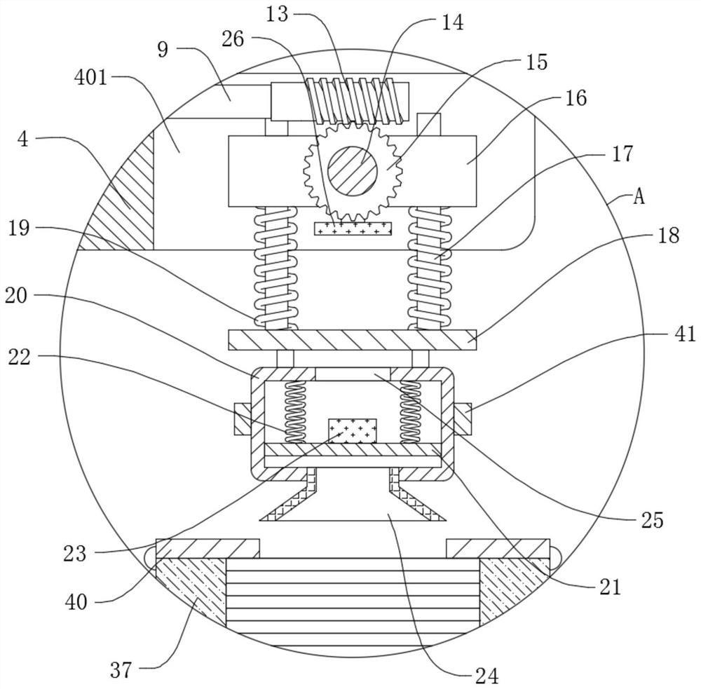
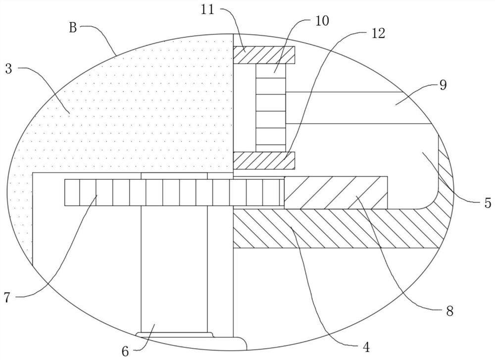
[0040]The detection mechanism includes a mounting groove 5 provided on the inner side wall of the rotating block 4. The mounting groove 5 is an annular groove. The gear 7 meshes, the number of teeth of the inner ring gear 8 is eight times the number of teeth of the first gear 7, and the number of teeth of the inner ring gear 8 is eight times the number of teeth of the first gear 7, ...


PUM


Abstract

An integrated circuit chip flatness detection device disclosed by the present invention comprises a machine base, a stand column is welded on the upper surface of the machine base, the stand column is fixedly connected with a fixed block, the side wall of the fixed block is fixedly connected with a plurality of detectors, and the fixed block is rotatably connected with a rotating block through a bearing in a penetrating manner. A detection mechanism for flatness detection is arranged in the rotating block; the detection mechanism comprises a mounting groove formed in the inner side wall of the rotating block, the inner bottom wall of the mounting groove is fixedly connected with an inner gear ring, the inner side wall of the fixed block is fixedly connected with a servo motor through a support, an output shaft of the servo motor is in interference fit with a first gear, and the first gear is meshed with the inner gear ring; the rotating block is provided with eight functional grooves. Compared with the prior art, the chip detection device has the advantages that chips can be continuously and automatically detected, feeding, discharging and classification can be automatically carried out, and therefore the detection efficiency is greatly improved, and meanwhile the equipment cost and the labor cost are reduced.

Description

technical field [0001] The invention relates to the technical field of chip detection, in particular to an integrated circuit chip flatness detection device and method. Background technique [0002] Whether it is an electrical product or other electronic products, the integrated circuit is one of the important internal components. The integrated circuit is a kind of miniature electronic device or component. Using a certain process, the transistors, resistors, capacitors, inductors and other components required in a circuit are interconnected, and they are fabricated on a small or several small semiconductor wafers or dielectric substrates, and then packaged in a tube. , become a microstructure with the required circuit function, and the carrier of the integrated circuit is the chip. After the chip is produced, workers need to test the thickness and pin flatness of the semiconductor chip after production, so as to facilitate the subsequent use of the semiconductor chip. ; ...

Claims


Application Information

Patent Timeline
Patent Type & Authority Applications(China)
IPC IPC(8): B07C5/34B07C5/02B07C5/36B07C5/38
CPCB07C5/34B07C5/02B07C5/362B07C5/38
Inventor 李晓伟李晓杰
Owner 深圳市通恒伟创科技有限公司
Why Eureka
Try Eureka