Chip packaging structure with electromagnetic shielding function and packaging method

An electromagnetic shielding and chip packaging technology, applied in circuits, electrical components, transportation and packaging, etc., can solve the problems of electronic equipment not working properly, not having electromagnetic shielding function, lack of chip packaging technology, etc., to reduce equipment failure to work properly. Or the effect of failure, not easy to electromagnetic interference, not easy to damage the chip

Active Publication Date: 2022-06-03
GUANGDONG CHIPPACKING TECH
View PDF6 Cites 0 Cited by
  • Summary
  • Abstract
  • Description
  • Claims
  • Application Information

AI Technical Summary

Problems solved by technology

[0002] With the popularization of electronic equipment, the demand for chips used to realize circuit control or specific functions has increased significantly; production has also increased, but product performance is uneven; Among them, there is no electromagnetic shielding function, which makes the chip very prone to failure and the electronic equipment cannot work normally; therefore, there is a lack of a chip packaging process with electromagnetic shielding function

Method used


Image

  • Chip packaging structure with electromagnetic shielding function and packaging method
  • Chip packaging structure with electromagnetic shielding function and packaging method
  • Chip packaging structure with electromagnetic shielding function and packaging method

Examples


Embodiment Construction

[0024] The preferred embodiments of the present invention will be described below with reference to the accompanying drawings. It should be understood that the preferred embodiments described herein are only used to illustrate and explain the present invention, but not to limit the present invention.

[0025] according to Figure 1-6 As shown, an embodiment of the present invention provides a chip packaging method with an electromagnetic shielding function, including the following steps:

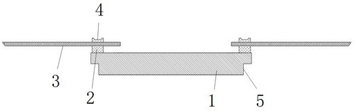
Prepare a heat sink 1 with insulating bumps 2, and bond metal pins 3 on the insulating bumps 2;

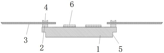
Adhere the chip module 6 to the side of the heat sink 1 with the insulating protrusion 2;

Use the wire harness to electrically connect the pins of the chip module 6 and the metal pins 3 on the insulating protrusions 2;

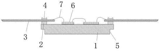
The shielding shell 8 is welded to the end of the insulating protrusion 2 away from the heat sink 1 , and the shielding shell 8 and the heat sink 1 are plastic-sealed to obtain ...


PUM


Abstract

The invention provides a chip packaging method with an electromagnetic shielding function, and the method comprises the following steps: preparing a cooling fin with an insulating projection, and bonding a metal pin on the insulating projection; bonding a chip module on one surface of the radiating fin, which is provided with the insulating bulge; the pins of the chip module are electrically connected with the metal pins on the insulating protrusions through wire harnesses; and welding a shielding shell at one end, far away from the radiating fin, of the insulating bulge, and carrying out plastic packaging on the shielding shell and the radiating fin to obtain a chip finished product. In the chip manufacturing process, the production and preparation technology is improved, so that the chip can have an electromagnetic shielding function, the product performance is further improved, and the situation that equipment cannot work normally or breaks down due to the fact that the chip is prone to being interfered by electromagnetic interference in the working process is reduced.

Description

technical field [0001] The invention relates to the technical field of chip packaging, in particular to a chip packaging structure and packaging method with electromagnetic shielding function. Background technique [0002] With the popularization of electronic equipment, the demand for chips used to realize circuit control or specific functions has increased significantly; the production volume has also increased, but the product performance is uneven; for example, the existing chips are used in the actual use process. It does not have the electromagnetic shielding function, so that the chip is very prone to failure and the electronic equipment cannot work normally; therefore, there is a lack of a chip packaging process that can have the electromagnetic shielding function. SUMMARY OF THE INVENTION [0003] The invention provides a chip packaging structure and packaging method with electromagnetic shielding function, which are used to improve the production and preparation ...

Claims


Application Information

Patent Timeline
Patent Type & Authority Applications(China)
IPC IPC(8): H01L21/52H01L21/56H01L21/67H01L21/677H01L23/552H01L23/31H01L23/367
CPCH01L21/52H01L21/56H01L23/552H01L23/3672H01L23/3107H01L21/67121H01L21/67721H01L21/67259
Inventor 程浪陈勇张怡饶锡林黄乙为
Owner GUANGDONG CHIPPACKING TECH
Why Eureka
Try Eureka