Photosensitive sensor, manufacturing method thereof and movable platform

A photosensitive sensor and photosensitive area technology, applied in the field of photosensitive sensors, can solve the problems of low quantum absorption efficiency, low sensor performance, weak infrared light absorption ability, etc., to increase the probability of photons being absorbed, high quantum absorption efficiency, and improve detection. Effects of Accuracy and Detection Range

Pending Publication Date: 2022-06-17
SZ DJI TECH CO LTD
View PDF0 Cites 0 Cited by
  • Summary
  • Abstract
  • Description
  • Claims
  • Application Information

AI Technical Summary

Problems solved by technology

[0003] Silicon-based APDs are widely used, but due to the properties of silicon itself, its ability to absorb infrared light with longer wavelengths is weak, and a thicker active absorption region is required to have better quantum absorption efficiency (QE), while It is difficult to form a thicker active absorption region in the usual semiconductor process. Due to the insufficient thickness of the active absorption region, the quantum absorption efficiency is low, generally difficult to exceed 15%, and the sensor performance is low, which limits its application.

Method used


Image

  • Photosensitive sensor, manufacturing method thereof and movable platform
  • Photosensitive sensor, manufacturing method thereof and movable platform
  • Photosensitive sensor, manufacturing method thereof and movable platform

Examples


Embodiment Construction

[0033] The technical solutions in the embodiments of the present application will be clearly and completely described below with reference to the accompanying drawings in the embodiments of the present application. Obviously, the described embodiments are part of the embodiments of the present application, not all of the embodiments. Based on the embodiments in this application, all other embodiments obtained by those of ordinary skill in the art without creative efforts shall fall within the protection scope of this application.

[0034] The flowcharts shown in the figures are for illustration only, and do not necessarily include all contents and operations / steps, nor do they have to be performed in the order described. For example, some operations / steps can also be decomposed, combined or partially combined, so the actual execution order may be changed according to the actual situation.

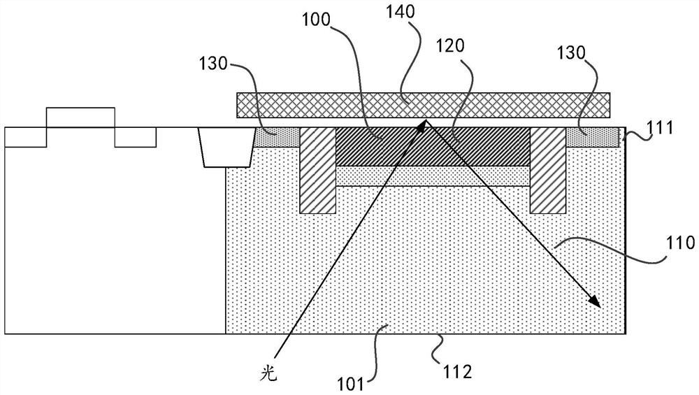
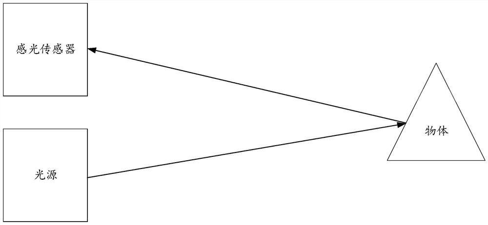
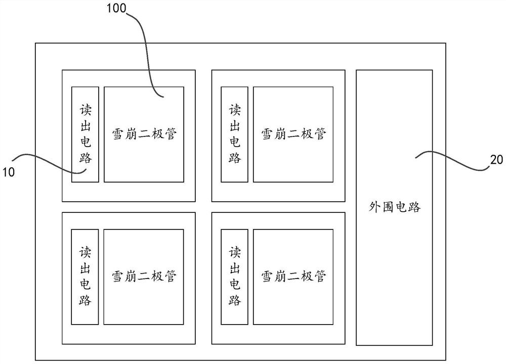
[0035] Some embodiments of the present application will be described in detail below wi...


PUM


Abstract

The photosensitive sensor comprises one or more avalanche diodes, each avalanche diode comprises an active photosensitive region, a first doped region and a second doped region, the active photosensitive region is provided with a first side and a second side opposite to the first side, and the second side is provided with a light incident surface; and the first reflective structure is close to the first side, is arranged opposite to the first doped region and the second doped region, and is used for reflecting light from the active photosensitive region back to the active photosensitive region. The photosensitive sensor provided by the invention has relatively high quantum absorption efficiency. The invention also provides a manufacturing method and a movable platform.

Description

technical field [0001] The present application relates to the technical field of photosensitive sensors, and in particular, to a photosensitive sensor, a manufacturing method thereof, and a movable platform. Background technique [0002] Sensors using avalanche diodes (APDs), such as time-of-flight sensors (TOFs), are widely used in consumer electronics, security monitoring, industrial automation, artificial intelligence, Internet of Things and other fields to collect and organize spatial distance data information for subsequent processing. and applications provide a source of information. [0003] Silicon-based APDs are widely used, but due to the properties of silicon itself, its ability to absorb infrared light with longer wavelengths is weak, and a thicker active absorption region is required to have better quantum absorption efficiency (QE). It is difficult to form a thick active absorption region in the usual semiconductor process. Due to the insufficient thickness of...

Claims


Application Information

Patent Timeline
IPC IPC(8): H01L31/0216H01L31/107H01L31/18H01L27/144G01S17/02
CPCH01L31/02161H01L31/107H01L31/18H01L27/1443H01L27/1446G01S17/02H01L31/0216H01L27/144H01L27/146
Inventor 徐泽肖琳占世武
Owner SZ DJI TECH CO LTD
Why Eureka
Try Eureka