
High-frequency high-power packaging module and manufacturing method thereof

A high-power, mold-loading technology, which is applied in semiconductor/solid-state device manufacturing, semiconductor/solid-state device components, semiconductor devices, etc., can solve the problem of increased loop inductance, achieve the effect of reducing loop inductance and ensuring heat dissipation

Inactive Publication Date: 2022-06-24
SHANGHAI METAPWR ELECTRONICS CO LTD +1
View PDF0 Cites 3 Cited by
  • Summary
  • Abstract
  • Description
  • Claims
  • Application Information

AI Technical Summary

Problems solved by technology

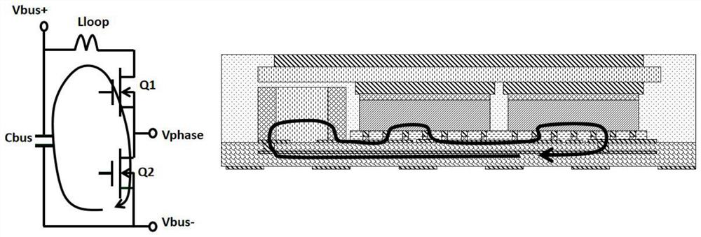
Due to the existence of wirebond, the loop inductance is greatly increased, which limits the increase in switching speed, which also limits the increase in frequency.

Method used


Image

  • High-frequency high-power packaging module and manufacturing method thereof
  • High-frequency high-power packaging module and manufacturing method thereof
  • High-frequency high-power packaging module and manufacturing method thereof

Examples


Embodiment Construction

[0169] The technical solutions in the embodiments of the present invention will be clearly and completely described below with reference to the accompanying drawings in the embodiments of the present invention. Obviously, the described embodiments are only a part of the embodiments of the present invention, but not all of the embodiments. Based on the embodiments of the present invention, all other embodiments obtained by those of ordinary skill in the art without creative efforts shall fall within the protection scope of the present invention.

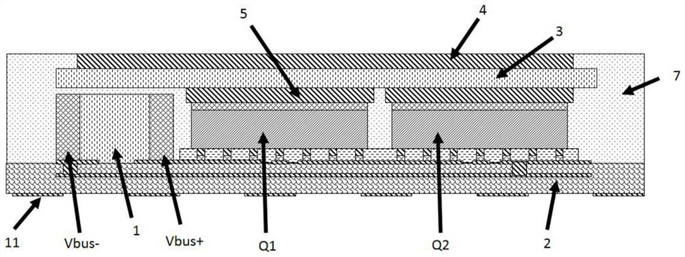
[0170] like Figure 2A and Figure 2BAs shown, the embodiment of the present invention discloses a high-frequency high-power packaging module, including at least one power conversion bridge arm and at least one high-frequency capacitor 1, the power conversion bridge arm includes at least two semiconductor power devices connected in series, and the high The frequency capacitor 1 is connected in parallel with the power conversion bridg...


PUM

PropertyMeasurementUnit
heightaaaaaaaaaa
heightaaaaaaaaaa

Abstract

The invention discloses a high-frequency high-power packaging module and a manufacturing method thereof, and the high-frequency high-power packaging module comprises at least one power conversion bridge arm, at least one high-frequency capacitor, a multi-layer circuit board, an insulating heat-conducting plate and a plastic package body. The back surface of the semiconductor power device is in thermal connection or electric connection with the lower surface of the insulating heat-conducting plate, and the high-frequency capacitor is electrically connected with the first surface of the multi-layer circuit board or the second surface of the multi-layer circuit board or the lower surface of the insulating heat-conducting plate. And at least one electrode of the high-frequency capacitor is electrically connected with at least one electrode of the at least one semiconductor power device through the inner electric connection layer. According to the invention, the heat dissipation capability is guaranteed, the loop inductance is greatly reduced, high power and high frequency are realized, the advantages of a third-generation semiconductor are fully played, and an application basis is provided for the upgrading of the performance of the third-generation semiconductor.

Description

technical field [0001] The invention belongs to the technical field of semiconductor packaging, and in particular relates to a high-frequency and high-power packaging module and a manufacturing method thereof. Background technique [0002] With the gradual maturity of the third-generation semiconductor GaN / SiC, its applications are becoming more and more extensive. Compared with traditional silicon devices, its equivalent internal resistance is greatly reduced, which greatly increases the applicable power of a single semiconductor power device. At the same time, the third-generation semiconductor also has better switching characteristics, its switching loss is greatly reduced, and it is easier to work at high frequencies. However, due to the deficiencies of the existing packaging technology, it is difficult to obtain the above two advantages at the same time. [0003] like figure 1 As shown in the figure, due to the small area and high thermal density of the semiconductor...

Claims


Application Information

Patent Timeline
Patent Type & Authority Applications(China)
IPC IPC(8): H01L23/34H01L21/48H01L23/367H01L23/495H01L23/498
CPCH01L23/367H01L23/3736H01L23/642H01L23/647H01L23/293H01L23/3107H01L23/40H01L21/50H01L23/373H01L23/32H01L2224/48247H01L2224/48137H01L2224/73265H01L2924/181H01L2224/97H01L2224/16225H01L2224/32225H01L2224/73204H01L2924/19105H01L2224/73253H01L2924/15192H01L2924/00012H01L2924/00
Inventor 曾剑鸿
Owner SHANGHAI METAPWR ELECTRONICS CO LTD
Learn More