Manufacturing method of electron emitter, electron source and image formation equipment

A technology of electron emission and manufacturing method, which is applied in the manufacture of discharge tubes/lamps, electrode systems, ships or lead wires, etc. It can solve the problems of electron beams not converging, poor image display performance, and substrate cracking, etc.

Inactive Publication Date: 2004-04-21
CANON KK
View PDF1 Cites 0 Cited by
  • Summary
  • Abstract
  • Description
  • Claims
  • Application Information

AI Technical Summary

Problems solved by technology

[0015] On the other hand, as a result of the above-mentioned energization forming process, the electron-emitting region produced in the surface conduction type electron-emitting device may become curved, especially when the distance between the device electrodes is large, thus reducing the Convergence of electron beams emanating from there
Thus, the energization forming process in the manufacture of surface conduction type electron-emitting devices is likely to lose accuracy in the position and cross-sectional facet of the electron-emitting region, resulting in devices with poor operability
[0016] Thus, in an electron source comprising a large number of surface conduction type electron-emitting devices with device electrodes separated by a large distance, and in an image forming apparatus using such an electron source, the electron-emitting operation of the electron-emitting devices is not uniform, Therefore, the distribution of brightness is also uneven, and the electron beams they emit cannot be converged in the desired way.
Since the device can only provide a blurry image, its image display performance must be poor
[0017] In addition, in the energization forming process for producing electron-emitting regions of surface conduction type electron-emitting devices, the power consumed by each device is generally between several tens of milliwatts and several hundred milliwatts. A single electron source for , or an imaging device using such an electron source requires a huge amount of power
Therefore, during the energization forming process, the voltage applied to each device produces a significant voltage drop, with additional loss of uniformity in the performance of the resulting devices
In some cases, the substrate may be cracked during actuation as a result of the lack of uniformity

Method used


Image

  • Manufacturing method of electron emitter, electron source and image formation equipment
  • Manufacturing method of electron emitter, electron source and image formation equipment
  • Manufacturing method of electron emitter, electron source and image formation equipment

Examples


Embodiment 1

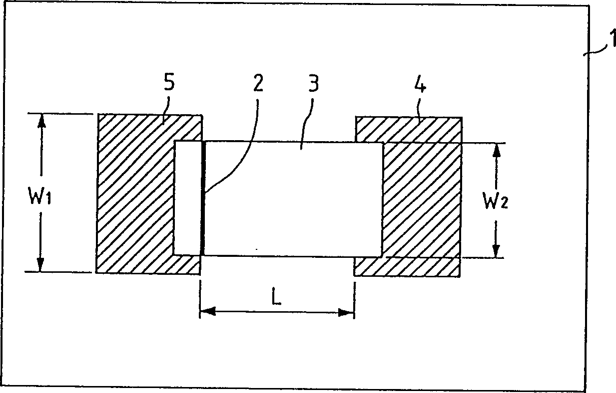
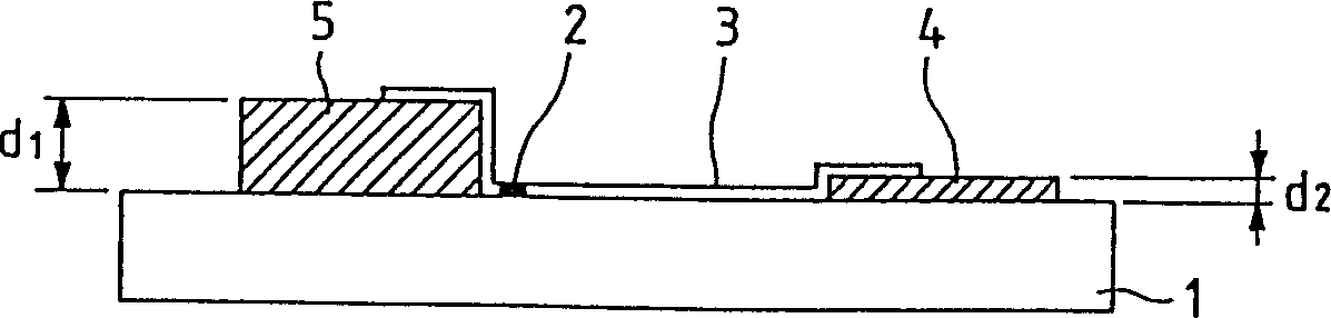
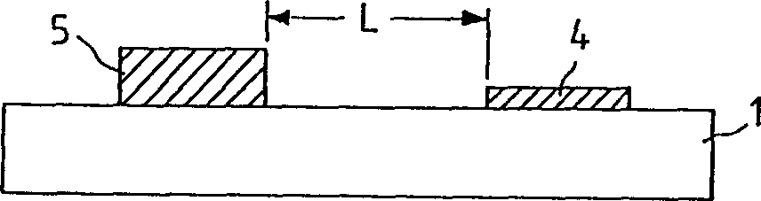
[0100] This embodiment is designed to show how Figure 1A and 1B Schematic illustration of the first basic structure. Note: Reference numerals 1, 2, and 3 denote the substrate, electron-emitting region, and conductive film including the electron-emitting region, respectively, and numerals 4 and 5 represent device electrodes.

[0101] Materials that can be used as the substrate 1 include quartz glass, glass containing a low concentration of impurities such as Na, and soda-lime glass on which a SiO 2 Layers, ceramic substances such as alumina and Si can constitute a glass substrate.

[0102] Although the opposite device electrodes 4 and 5 can be made of any highly conductive material, preferred materials include metals (such as: Ni, Cr, Au, Mo, W, Pt, Ti, Al, Cu, and Pb) and their Alloys from Pb, Ag, RuO 2 , Pd-Ag and metals or metal oxides selected from glass can be printed conductive materials, transparent conductive materials (such as In 2 o 3 -SnO 2 ), and semiconduct...

Embodiment 2

[0133] The second basic structure of the surface conduction type electron-emitting device according to the present invention will now be described.

[0134] in having Figure 4A and 4B In the surface conduction type electron-emitting device of the second basic structure shown, an electron-emitting region is formed adjacent to any one of a pair of device electrodes 4 and 5, and the heights of the respective stepped portions of the device electrodes 4 and 5 are equal to each other.

[0135] Such as Figure 4A and 4B As shown, a conductive thin film 3 is formed on a device electrode 5 and below another device electrode 4 . Therefore, only a step is produced on the device electrode 5 on the conductive film, and thus an electron-emitting region 2 is formed after the energization forming process at a position close to the device 5 .

[0136] As described above with reference to the first embodiment, the relationship between the height of the device electrode 5 and the conductive...

Embodiment 3

[0145] In the surface conduction type electron-emitting device according to the present invention, any one of the pair of device electrodes (in the Figure 1A and 1B An electron emission region 2 is formed at the position of the device electrode 5). Such an electron-emitting region 2 can be produced by any one of the first and second manufacturing methods according to the present invention, which will be described in more detail below.

[0146] Refer below Figures 2A to 2C described as Figure 1A and 1B Said surface conduction type electron-emitting device according to the present invention, Figures 2A to 2C Such devices are represented at different fabrication steps.

[0147] 1) After the substrate 1 is thoroughly cleaned with detergent and pure water, a material is deposited on the substrate 1 by vacuum deposition, sputtering, or some other suitable technique to obtain a pair of device electrodes 4 and 5, The device electrodes 4 and 5 are then produced by photolithog...


PUM


Abstract

To provide a manufacturing method of an electron emission element which comprises a conductive thin film that includes an electron-emitting region disposed between a pair of electrodes arranged on a substrate. The method comprises the process wherein an organometal solution containing component elements for the conductive thin film is sprayed to the substrate through the nozzle while potential being kept different between the electrodes. This invention also involves a manufacture method of an electron source and a manufacture method of imaging device.

Description

technical field [0001] This application is a divisional application of the Chinese patent application with the application number 95117385.5 and the invention title "Electron emission device and its manufacturing method, electron source and imaging device" submitted by the applicant on September 22, 1995. [0002] The present invention relates to a novel electron-emitting device, and also relates to an image forming apparatus and an electron source including such an electron-emitting device. Background technique [0003] There are two types of electron-emitting devices in the prior art: thermionic cathode devices and cold cathode devices. Cold cathode devices refer to field emission type (hereinafter referred to as FE type), metal / insulation layer / metal type (hereinafter referred to as MIM type), surface conduction type, etc. > Examples of FE type devices include: W.P.Dyke and W.W.Dolen in the article entitled "Field Emis-sion" (Advance in Electron Physics, 8, 89 (1956))...

Claims


Application Information

Patent Timeline
Patent Type & Authority Patents(China)
IPC IPC(8): G09G3/22H01J1/316H01J9/02
CPCG09G3/22H01J9/027H01J2201/3165H01J2329/00H01J1/316H01J1/30H01J9/24
Inventor 山野边正人塚本健夫山本敬介浜元康弘
Owner CANON KK
Why Eureka
Try Eureka