Semiconductor light emitting element
A technology of light-emitting elements and semiconductors, which is applied in the direction of semiconductor devices, electrical components, circuits, etc., and can solve the problems of inability to inject light-emitting elements and fully luminous light-emitting elements
- Summary
- Abstract
- Description
- Claims
- Application Information
AI Technical Summary
Problems solved by technology
Method used
Image

Examples
Embodiment 1
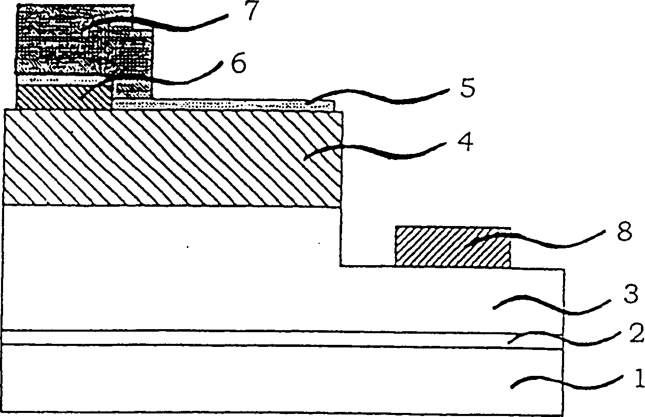
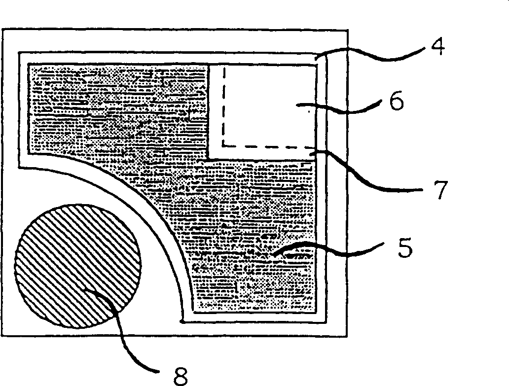
[0040] 1( a ) and ( b ) show the electrode structure of the gallium nitride-based compound semiconductor light-emitting device of the present invention.
[0041] This light-emitting device is a p-type gallium nitride that forms a light-emitting surface by sequentially stacking a buffer layer 2, an n-type gallium nitride-based compound semiconductor layer 3, and a p-type gallium nitride-based compound semiconductor layer 4 on an insulating substrate. A current blocking layer 6 and a light-transmitting electrode 5 are formed on the compound semiconductor layer 4, and a pad electrode 7 having an electrode connection portion connected to the light-transmitting electrode 5 is formed on the current blocking layer 6. The n-type gallium nitride-based compound semiconductor An n-type electrode 8 is formed on layer 3 .
[0042] Next, a method of manufacturing the above-mentioned light-emitting element will be described.
[0043] First, an AlGaN buffer layer 2 , an n-type gallium nitrid...
Embodiment 2
[0053] Another GaN-based compound semiconductor light-emitting element of the present invention is shown in figure 2 .
[0054] This light-emitting element is formed by sequentially laminating an AlGaN buffer layer 2, a p-type gallium nitride-based compound semiconductor layer 4, and an n-type gallium nitride-based compound semiconductor layer 3 on an insulating substrate 1 to form an n-type nitrogen oxide layer on the light-emitting surface. A current blocking layer 6 made of silicon nitride, a light-transmitting electrode 5 made of titanium, and a pad electrode 7 are formed on the gallium-based compound semiconductor layer 3 .
[0055] A method of manufacturing such a light-emitting element will be described below.
[0056] First, an AlGaN buffer layer 2 , a p-type gallium nitride-based compound semiconductor layer 4 , and an n-type gallium nitride-based compound semiconductor layer 3 are stacked on a sapphire substrate 1 .
[0057] Next, a silicon nitride current blockin...
Embodiment 3
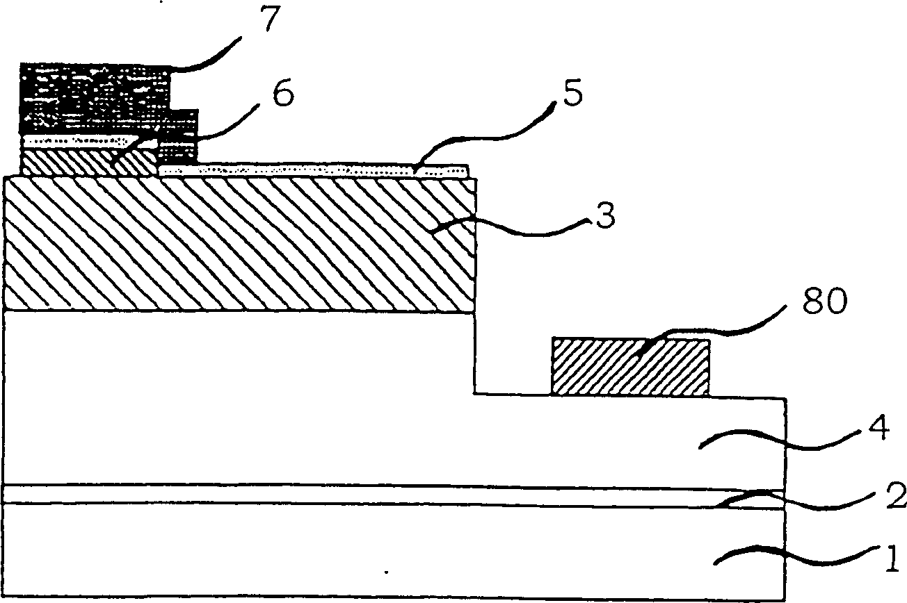
[0065] 3( a ) and ( b ) show yet another gallium nitride-based compound semiconductor light-emitting device of the present invention.
[0066] In Example 3, the n-type gallium nitride-based compound semiconductor layer 3 and the p-type gallium nitride-based compound semiconductor layer 4 are sequentially stacked on the n-type conductive substrate 60 to form the p-type gallium nitride-based compound semiconductor layer 4 on the light emitting surface. A current blocking layer 6 made of titanium oxide and a light-transmitting electrode 5 are formed on the compound semiconductor layer 4, and a pad electrode 7 having an electrode connection portion in contact with the light-transmitting electrode 5 is formed on the upper surface of the current blocking layer 6 and its peripheral portion, An n-type electrode 8 is also formed on the back surface of the n-type conductive substrate 60 .
[0067] Next, a method of manufacturing the above-mentioned light-emitting element will be describ...
PUM
 Abstract
Description
Claims
Application Information
 - R&D
- Intellectual Property
- Life Sciences
- Materials
- Tech Scout
- Unparalleled Data Quality
- Higher Quality Content
- 60% Fewer Hallucinations
Browse by: Latest US Patents, China's latest patents, Technical Efficacy Thesaurus, Application Domain, Technology Topic, Popular Technical Reports.
© 2025 PatSnap. All rights reserved.Legal|Privacy policy|Modern Slavery Act Transparency Statement|Sitemap|About US| Contact US: help@patsnap.com