Input stage circuit and amplifier

An input stage and circuit technology, which is applied in the direction of amplifier protection circuit layout, improved amplifiers to expand bandwidth, improved amplifiers to reduce noise impact, etc., can solve the problems of limiting the closed-loop bandwidth, stability and noise performance of transimpedance amplifiers, and achieve improved Closed-loop bandwidth, reducing equivalent input capacitance, and suppressing the effect of charging and discharging

Pending Publication Date: 2022-07-05
3PEAK (SHANGHAI) LTD
View PDF0 Cites 0 Cited by
  • Summary
  • Abstract
  • Description
  • Claims
  • Application Information

AI Technical Summary

Problems solved by technology

In transimpedance closed-loop applications of high-speed, low-noise amplifiers, large input capacitance limits the closed-loop bandwidth, stability, and noise performance of the transimpedance amplifier

Method used


Image

  • Input stage circuit and amplifier
  • Input stage circuit and amplifier
  • Input stage circuit and amplifier

Examples


Embodiment 1

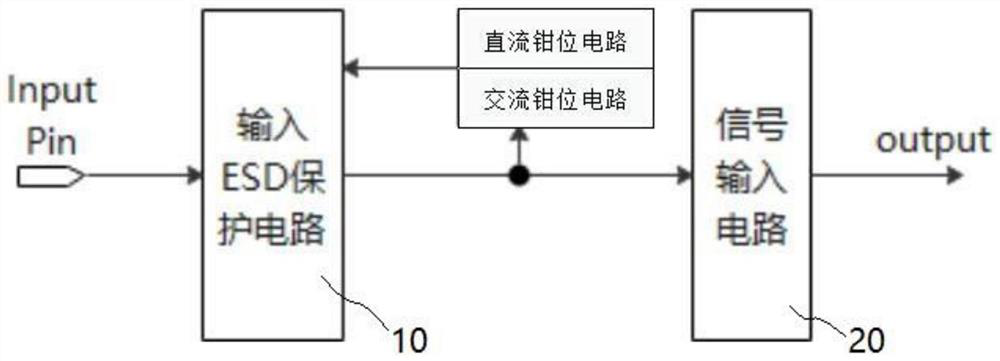
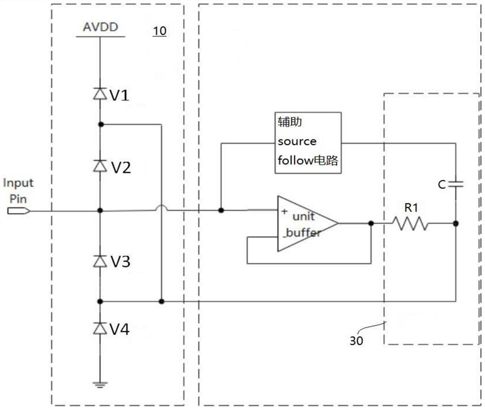
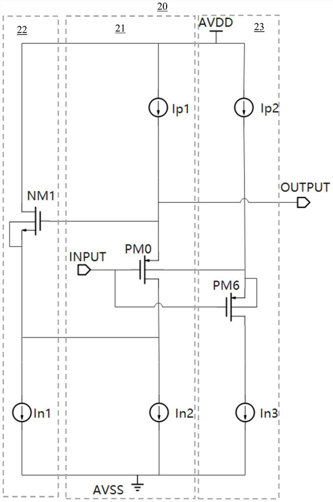
[0032] like figure 1 , figure 2 and image 3 As shown, an input stage circuit includes: an input ESD protection circuit 10 , a DC clamp circuit, an AC clamp circuit and a signal input circuit 20 which are connected. The DC clamp circuit includes a unit buffer. The AC clamp circuit includes an auxiliary source follower circuit and a high-pass filter circuit 30 . The signal input circuit 20 includes a main source follower circuit 21 , a first sub-source follower circuit 22 and a second sub-source follower circuit 23 connected to the main source follower circuit 21 .

[0033] The DC clamp circuit and the AC clamp circuit are used to reduce the equivalent input capacitance of the input ESD protection circuit 10 . Through the DC clamp circuit and the AC clamp circuit, the voltages across the parasitic capacitances of the devices input to the ESD protection circuit 10 can follow each other, that is, the voltage difference across the parasitic capacitances of the devices input t...


PUM


Abstract

The input stage circuit comprises an input ESD protection circuit, a direct current clamping circuit and an alternating current clamping circuit which are connected, and the alternating current clamping circuit comprises an auxiliary source follow circuit and a high-pass filter circuit which are connected with the input ESD protection circuit and the direct current clamping circuit. And the direct current clamping circuit, the auxiliary source follow circuit and the high-pass filter circuit are used for reducing equivalent input capacitance input into the ESD protection circuit. According to the input stage circuit provided by the embodiment of the invention, through the direct current clamping circuit and the alternating current clamping circuit, the voltages at the two ends of the parasitic capacitors of all devices input into the ESD protection circuit follow each other, the charge and discharge of the parasitic capacitors in the signal input process are inhibited, and the equivalent input capacitance of the input stage circuit is reduced; and the closed-loop bandwidth, the stability and the noise performance of the trans-impedance amplifier are greatly improved.

Description

technical field [0001] The present invention relates to the field of integrated circuits, in particular to an input stage circuit and an amplifier. Background technique [0002] The input capacitance of the amplifier comes from the parasitic capacitance of the internal input ESD protection circuit and the gate-source, gate-drain, gate-substrate and drain-source of the input stage MOS transistor. parasitic capacitance between. In high-speed, low-noise amplifier transimpedance closed-loop applications, large input capacitance can limit the transimpedance amplifier's closed-loop bandwidth, stability, and noise performance. [0003] The information disclosed in this Background section is only for enhancement of understanding of the general background of the invention and should not be taken as an acknowledgement or any form of suggestion that this information forms the prior art already known to a person of ordinary skill in the art. SUMMARY OF THE INVENTION [0004] The pur...

Claims


Application Information

Patent Timeline
Patent Type & Authority Applications(China)
IPC IPC(8): H03F1/42H03F1/26H03F1/52
CPCH03F1/42H03F1/26H03F1/52
Inventor 张睿
Owner 3PEAK (SHANGHAI) LTD
Why Eureka
Try Eureka