Normally-off channel modulation device and manufacturing method thereof

A channel modulation and normally-off technology, applied in the field of microelectronics, can solve the problems of low device manufacturing yield, increase device parasitic capacitance, attenuate device frequency characteristics, etc., achieve simple manufacturing process, good output characteristics, and improve manufactured products rate effect

Pending Publication Date: 2021-12-31
XIDIAN UNIV
View PDF2 Cites 0 Cited by
  • Summary
  • Abstract
  • Description
  • Claims
  • Application Information

AI Technical Summary

Problems solved by technology

However, the manufacturing process of GaN-based normally-off power switching devices using field plate technology is relatively complicated, and the device manufacturing yield is low, resulting in high manufacturing costs.
In addition, the use of field plate technology will also increase the parasitic capacitance of the device, thereby attenuating the frequency characteristics of the device

Method used


Image

  • Normally-off channel modulation device and manufacturing method thereof
  • Normally-off channel modulation device and manufacturing method thereof
  • Normally-off channel modulation device and manufacturing method thereof

Examples


Embodiment 1

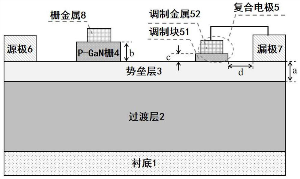
[0057] Example 1: Making the barrier layer 3 thickness in the sapphire substrate is 1 nm, the modulation block 51 doped concentration is 5 × 10 15 cm -3 The thickness is 1 nm, the horizontal distance D = 0 μm of the right end and the left end of the drain 7 is D = 0 μm.

[0058] Step 1. Upper excess GaN material production transition layer 2 in sapphire substrate 1, such as Figure 4 a.

[0059] 1A) GaN material using metal organic chemical vapor deposition techniques at the sapphire substrate 1 is 30 nm, the process conditions are: the temperature is 500 ° C, the pressure is 46 torr, the hydrogen flow is 4300 sccm, the ammonia gas flow is 4300 sccm, gallium The source flow is 21μmol / min;

[0060] 1B) The use of metal organic chemical vapor deposition techniques at GaN material having a thickness of 0.47 μm in GaN material, forming an undoped transition layer 2, wherein the process conditions are: temperature is 960 ° C, the pressure is 45 torr, and the hydrogen flow is 4400 sccm...

Embodiment 2

[0081] Example 2: Making the barrier layer 3 thickness at the silicon substrate is 25 nm, the modulation block 51 doped concentration is 1 × 10 22 cm -3 The thickness is 5 nm, the horizontal distance between the right end of the modulation block 51 and the left end of the drain 7, D = 2 μm.

[0082] Step 1. On the silicon substrate 1, the upper epitaxial Aln and GaN material make transition layer 2, such as Figure 4 a.

[0083] 1.1) Use metal organic chemical vapor deposition techniques at temperatures of 820 ° C, the pressure is 42 torr, the hydrogen flow is 4300 sccm, the ammonia gas flow is 4300 sccm, and the aluminum source is from 21 μmol / min, on the silicon substrate 1. ALN material having a thickness of 300 nm;

[0084] 1.2) Use metal organic chemical gas phase deposition techniques at temperatures of 970 ° C, the pressure is 44 torr, the hydrogen flow is 4400 sccm, the ammonia gas flow is 4400 sccm, and the gallium source flow is 110 μmol / min, and the ALN material is e...

Embodiment 3

[0098] Example Three: a silicon carbide substrate formed on the barrier layer 3 having a thickness of 20nm, the modulation block 51 doping concentration of 6 × 10 18 cm -3 And a thickness of 2.3 nm, and the horizontal distance between a right end of the left end of the drain modulation block 7 to 51 d = channel normally-off modulation device of 3μm.

[0099] Step A. bottom-up on the silicon carbide substrate 1 and the GaN epitaxial material AlN buffer layer 2, such as Figure 4 a.

[0100] A1) setting a temperature of 1050 ℃, pressure of 46Torr, a hydrogen flow rate of 4600sccm, ammonia flow rate of 4600sccm, the aluminum source flow was 6μmol / min, using a metal organic chemical vapor deposition technique in a thickness of epitaxial silicon carbide on the substrate is 90nm the AlN material;

[0101] A2) setting a temperature of 1050 ℃, pressure of 46Torr, a hydrogen flow rate of 4600sccm, ammonia flow rate of 4600sccm, flow rate of the gallium source 100μmol / min, using a metal ...


PUM

PropertyMeasurementUnit
thicknessaaaaaaaaaa
thicknessaaaaaaaaaa
thicknessaaaaaaaaaa

Abstract

The invention discloses a normally-off channel modulation device and a manufacturing method thereof, which mainly solve the problem of current collapse of the existing gallium nitride-based power switch device. The normally-off channel modulation device comprises a substrate (1), a transition layer (2) and a barrier layer (3) from bottom to top, wherein a source electrode (6), a P-GaN gate (4), a composite electrode (5) and a drain electrode (7) are sequentially arranged on the barrier layer (3) from left to right, and gate metal (8) is deposited on the upper part of the P-GaN gate (4). The composite electrode (5) is composed of a lower modulation block (51) and an upper modulation metal (52), and the thickness of the modulation block (51) is smaller than that of the P-GaN gate (4) so as to ensure that two-dimensional electron gas in a channel formed between a barrier layer and a transition layer at the lower part of the modulation block (51) is almost not exhausted in an equilibrium state. The modulation metal (52) is electrically connected to the drain (7). The device can effectively inhibit the current collapse of the normally-off device, and can be used for a basic device of a power electronic system.

Description

Technical field [0001] The present invention belongs to the field of microelectronics, and in particular, to a typical channel modulation device, which can be used as a basic device as a power electronics system. [0002] technical background [0003] Currently, vigorously develop high-performance, high-reliability power switching devices to significantly improve the efficiency and overall performance of the power electronic system, one of the effective ways to help energy conservation and emission reduction and green development strategy. The traditional silicon-based power switching device is limited by the silicon material itself, its performance has approached the theoretical limit, and the next-generation power electronics system is not met with high temperature, high pressure, high frequency, efficient and high power density requirements. The gallium nitride-based power switching device, especially the tympanic high electron mobility device based on the p-type cap layer GaN ...

Claims


Application Information

Patent Timeline
Patent Type & Authority Applications(China)
IPC IPC(8): H01L29/778H01L29/417H01L21/335
CPCH01L29/7787H01L29/41758H01L29/66462
Inventor 毛维裴晨杨翠杜鸣马佩军张鹏张进成郝跃
Owner XIDIAN UNIV
Why Eureka
Try Eureka