Semiconductor MEMS packaging structure and method
A packaging structure and semiconductor technology, applied in semiconductor devices, semiconductor/solid-state device parts, microstructure technology, etc., can solve problems such as poor chip working effect, achieve good working environment temperature, good cooling effect, and avoid heat generation hot effect
- Summary
- Abstract
- Description
- Claims
- Application Information
AI Technical Summary
Problems solved by technology
Method used
Image
Examples
Embodiment Construction
[0036] The present invention will be further described in detail below with reference to the accompanying drawings and embodiments, so that those skilled in the art can implement the invention with reference to the description.
[0037] It should be understood that terms such as "having", "comprising" and "including" as used herein do not exclude the presence or addition of one or more other elements or combinations thereof.
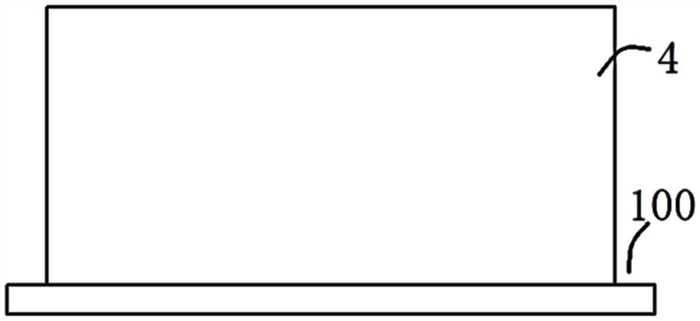
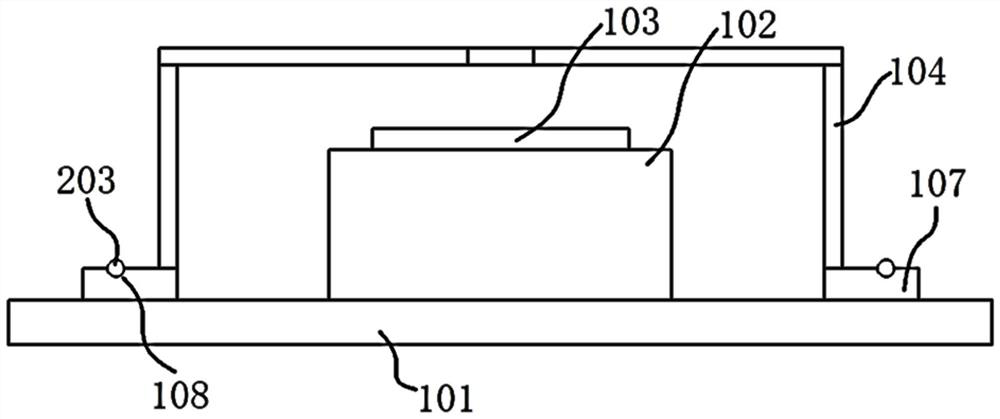
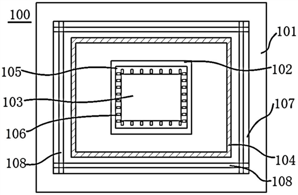
[0038] like Figure 1-Figure 11 As shown, the present invention provides a semiconductor MEMS package structure, including: a package structure body 100 and an anti-drop exhaust assembly 4, the package structure body 100 includes a substrate 101, a sensor group, and a cap body 104, the sensor group The cap body 104 is arranged on the substrate 101 and covered on the sensor group. The cap body 104 is provided with an exhaust hole, and the anti-fall exhaust The assembly 4 is disposed on the base plate 101 , and the cap body 104 is located in the anti-fall e...
PUM
 Abstract
Description
Claims
Application Information


