Neural network mapping method based on linear programming for storage and calculation integrated chip

A neural network and linear programming technology, applied in the field of semiconductors, can solve problems such as large noise, affecting operation accuracy, and increasing the scale of flash memory cell arrays, and achieve the effects of reducing numerical values, improving operation accuracy, and reducing current noise

Pending Publication Date: 2022-07-08
BEIJING ZHICUN WITIN TECH CORP LTD
View PDF0 Cites 2 Cited by
  • Summary
  • Abstract
  • Description
  • Claims
  • Application Information

AI Technical Summary

Problems solved by technology

In the tool chain design for memory-computing integrated chips, it is a key technology to automatically map the weight parameters of a specific neural network to the flash memory cell array of the chip according to requirements; When the flash memory cell array of the chip is on, the weights and biases are mapped to the memory-computing integrated chip array in turn according to the order of each layer of the neural network; however, this method cannot effectively utilize the flash memory cells on the one hand, and increases the scale of the flash memory cell array; On the other hand, since the bias is directly mapped to the memory-computing integrated chip array, the greater the value of the bias, the greater the conductance of the flash memory unit. Under the same voltage, the greater the current of the flash memory unit, the greater the noise and the Operational precision

Method used


Image

  • Neural network mapping method based on linear programming for storage and calculation integrated chip
  • Neural network mapping method based on linear programming for storage and calculation integrated chip
  • Neural network mapping method based on linear programming for storage and calculation integrated chip

Examples


Embodiment Construction

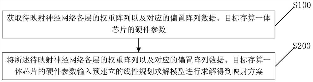
[0051] In order to make those skilled in the art better understand the solutions of the present application, the technical solutions in the embodiments of the present application will be clearly and completely described below with reference to the accompanying drawings in the embodiments of the present application. Obviously, the described embodiments are only The embodiments are part of the present application, but not all of the embodiments. Based on the embodiments in the present application, all other embodiments obtained by those of ordinary skill in the art without creative work shall fall within the scope of protection of the present application.

[0052] As will be appreciated by one skilled in the art, embodiments of the present invention may be provided as a method, system, or computer program product. Accordingly, the present invention may take the form of an entirely hardware embodiment, an entirely software embodiment, or an embodiment combining software and hardw...


PUM


Abstract

The embodiment of the invention provides a neural network mapping method based on linear programming for a storage and calculation integrated chip. The method comprises the following steps: acquiring a weight array of each layer of a neural network to be mapped, corresponding bias array data and hardware parameters of a target storage and calculation integrated chip; inputting the weight array of each layer of the neural network to be mapped, the corresponding bias array data and the hardware parameters of the target storage and calculation integrated chip into a pre-established linear programming solving model for solving to obtain a mapping scheme; the mapping scheme is used for mapping the weight array of each layer of the neural network to be mapped and the corresponding bias array to the target storage and calculation integrated chip. Wherein the calculation precision is improved by converting a weight and offset data mapping process based on visual experience into a solving problem of a mathematical model of linear programming.

Description

technical field [0001] The present invention relates to the technical field of semiconductors, and in particular, to a linear programming-based neural network mapping method, device, device and storage medium for a memory-computing integrated chip. Background technique [0002] In recent years, with the continuous development of the three dimensions of algorithm, computing power and data volume, machine learning technology continues to show strong advantages in solving many problems. Among them, artificial neural network has attracted extensive attention for its outstanding performance in image recognition, object detection, semantic segmentation and other fields. However, with the expansion of the scale of neural networks, the traditional mode of processing neural network algorithms with CPU+GPU architecture has gradually encountered bottlenecks in speed and power consumption. The centered neural network algorithm brings excessive data transmission overhead to the computin...

Claims


Application Information

Patent Timeline
Patent Type & Authority Applications(China)
IPC IPC(8): G06N3/063G06F17/10
CPCG06N3/063G06F17/10Y02D10/00
Inventor 胡剑超刘俊麟张爱飞
Owner BEIJING ZHICUN WITIN TECH CORP LTD
Why Eureka
Try Eureka