Etching processing equipment for semiconductor production

An etching processing, semiconductor technology, applied in semiconductor/solid-state device manufacturing, sustainable manufacturing/processing, final product manufacturing, etc., can solve the problem of inconvenient replacement of adsorption filter plates, easy diffusion of harmful gases, and difficulty in determining the saturation state of adsorption filter plates. and other problems, to achieve the effect of easy cleaning and increased sealing

Inactive Publication Date: 2022-07-12
江苏晶曌半导体有限公司
View PDF0 Cites 0 Cited by
  • Summary
  • Abstract
  • Description
  • Claims
  • Application Information

AI Technical Summary

Problems solved by technology

[0003] At present, the treatment and adsorption of harmful gases are mostly carried out at the output end of the conveyor belt. The equipment is mostly installed directly above the conveyor belt. There will be a gap between the side wall of the conveyor belt and the casing, and harmful gases are easy to diffuse out. There is no protection around the casing. The air is extracted from the structure, it is difficult to collect the harmful gas just released into the equipment, and the harmful gas is adsorbed through the adsorption filter plate. After a long time of use, it is difficult to determine whether the adsorption filter plate is in a saturated state, which is inconvenient. Replace the adsorption filter plate in time

Method used


Image

  • Etching processing equipment for semiconductor production
  • Etching processing equipment for semiconductor production
  • Etching processing equipment for semiconductor production

Examples


Embodiment Construction

[0028] In order to make it easy to understand the technical means, creative features, achieved goals and effects of the present invention, the present invention will be further described below with reference to the specific embodiments.

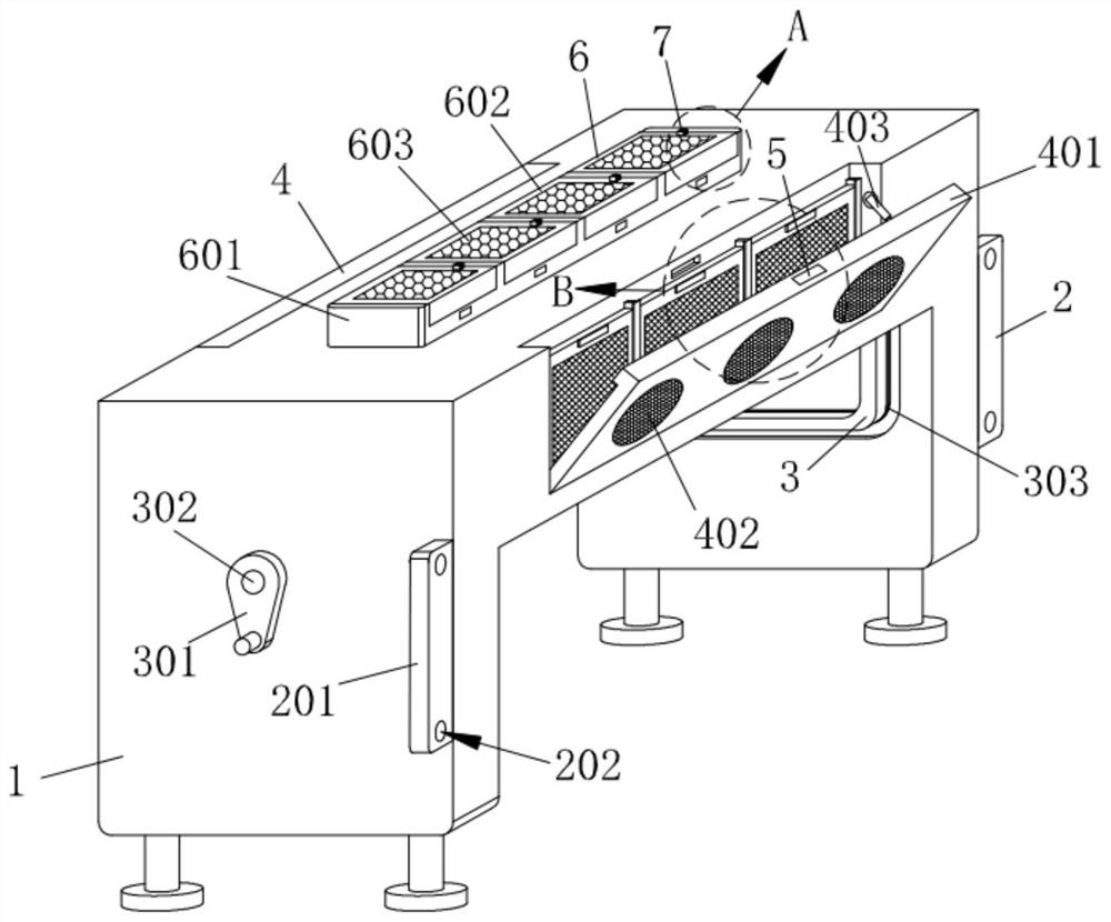
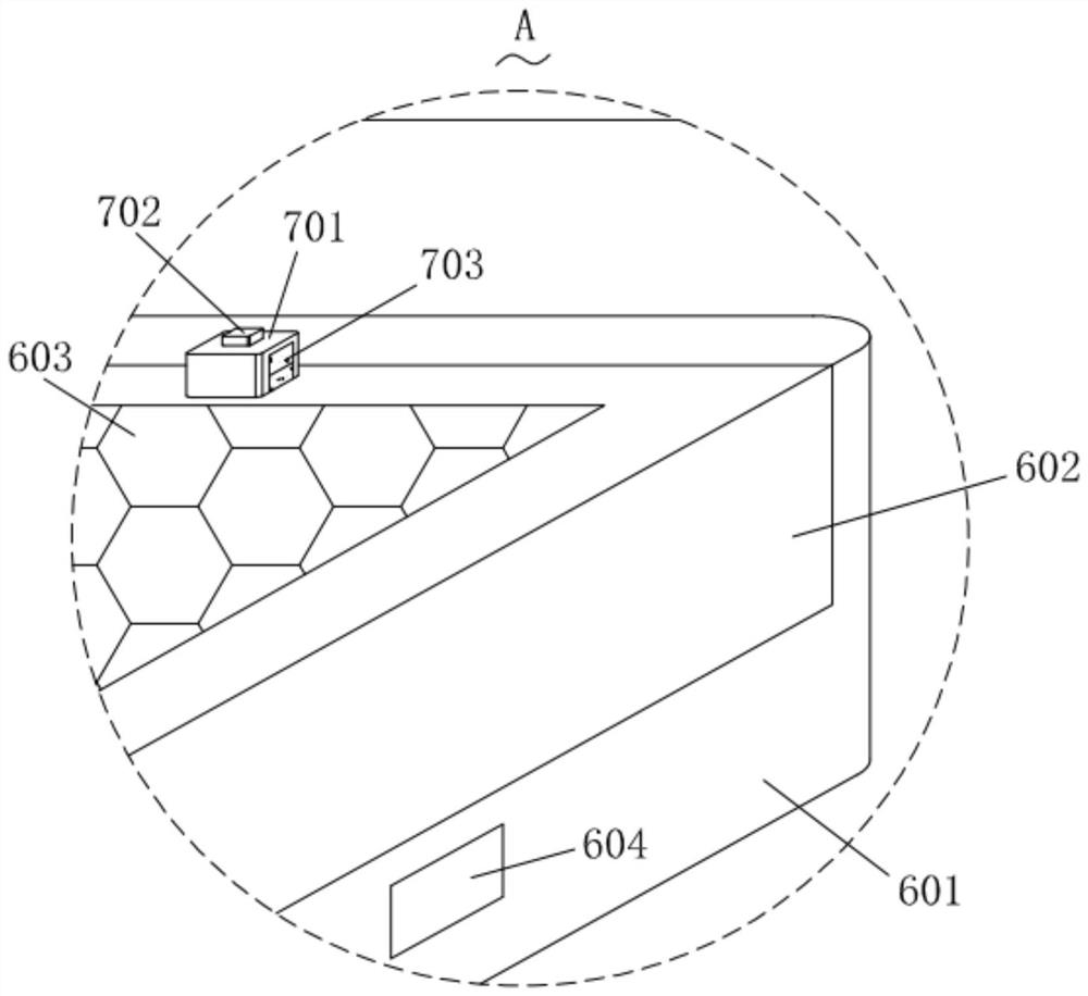
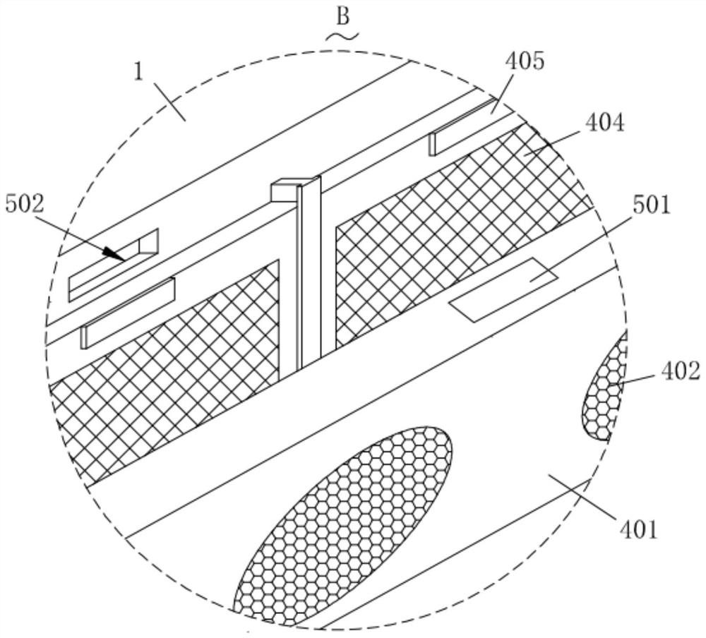
[0029] like Figure 1-Figure 10As shown, an etching processing equipment for semiconductor production according to the present invention includes a casing 1, on which is connected a mounting structure 2 for mounting and fixing, and on the casing 1 is connected a resistance for reducing the diffusion of harmful gases Structure 3, the casing 1 is connected with a suction structure 4 for collecting the scattered harmful gas, the suction structure 4 is connected with a limiting structure 5 for limiting the position, and the casing 1 is connected with a suction structure 5 for A filter structure 6 for adsorption and purification of harmful gases, the filter structure 6 is connected with an indicator structure 7 for indicating that it needs to be r...


PUM


Abstract

The invention relates to the technical field of semiconductors, in particular to etching processing equipment for semiconductor production, which comprises a shell, a mounting structure connected to the shell, an abutting structure connected to the shell, a suction structure connected to the shell, a limiting structure connected to the suction structure, and a filtering structure connected to the shell. The filtering structure is connected with an indicating structure; the shell can be conveniently installed and fixed to a conveying belt through the installation structure, the sealing performance can be improved through the abutting structure, emission of harmful gas in the shell is reduced, the harmful gas around the shell can be absorbed through the suction structure and the limiting structure, and the harmful gas on a semiconductor etching plate in the shell can be adsorbed and removed through the filtering structure; and whether the filtering structure is in a saturated state or not can be determined in time through the indication structure, and whether the filtering structure needs to be replaced or not is reminded.

Description

technical field [0001] The invention relates to the technical field of semiconductors, in particular to an etching processing equipment for semiconductor production. Background technique [0002] Semiconductors refer to materials with electrical conductivity between conductors and insulators at room temperature. Semiconductor etching plates will generate high-temperature harmful gases during etching. In order to prevent harmful gases from diffusing into the surrounding air and polluting the environment, it is necessary to deal with harmful gases. [0003] At present, the treatment and adsorption of harmful gases are mostly adopted at the output end of the conveyor belt, and the equipment is mostly installed directly above the conveyor belt. It is difficult to collect the newly released harmful gas into the equipment, and the harmful gas is adsorbed through the adsorption filter plate. It is difficult to determine whether the adsorption filter plate has been saturated after l...

Claims


Application Information

Patent Timeline
Patent Type & Authority Applications(China)
IPC IPC(8): B01D46/12B01D46/88H01L21/67
CPCB01D46/12B01D46/0036B01D46/0086H01L21/67063Y02P70/50
Inventor 白俊春程斌平加峰
Owner 江苏晶曌半导体有限公司
Why Eureka
Try Eureka