


Quick Research
Generate reliable direction feasibility study reports for your R&D in just a few steps.

Technical Q&A
Discover and master advanced knowledge NOW. Basics, ideas, possibilities, all at once.

Find Solutions
As an expert in R&D theories, this can generate solutions to your technical problems instantly.

Evaluate Feasibility
Analyze your overall solution with one click, know your potential R&D risks in advance.

Monitor Landscape
Get weekly tech updates, stay abreast of the latest tech innovations and key insights.
Supporting structure for semiconductor detection
A support structure and semiconductor technology, which is applied in the field of semiconductors, can solve the problems of measurement work influence, inaccurate measurement values, semiconductor damage, etc., and achieve the effect of increasing friction, reducing pressure, and facilitating movement
- Summary
- Abstract
- Description
- Claims
- Application Information
AI Technical Summary
Problems solved by technology
Method used
Image

Examples
Embodiment
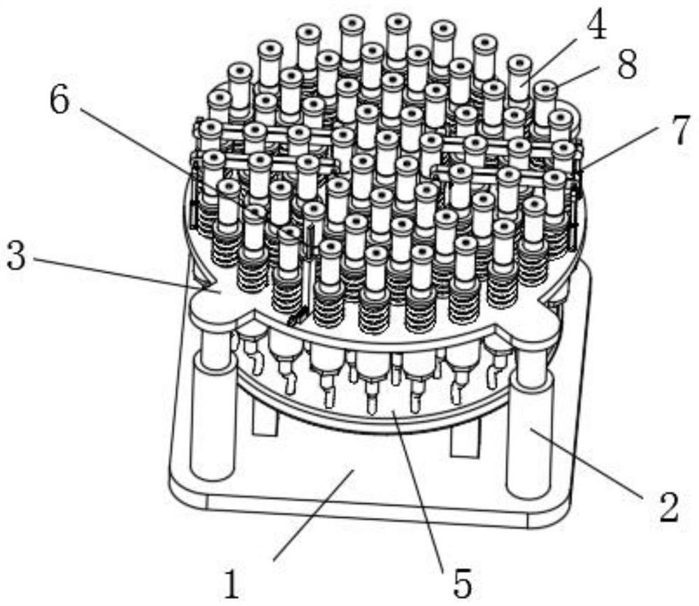
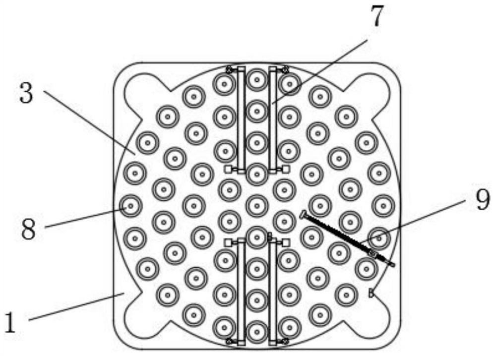
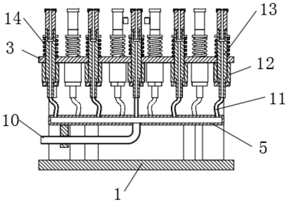
[0042] Example: Reference Figure 1-8 The shown support structure for semiconductor inspection includes a base plate 1, a fixed plate 3 is installed on the top side of the base plate 1 through a plurality of first telescopic rods 2, and a plurality of sliding holes 25 are opened on the fixed plate 3. 25 are slidably installed with pop-up units, the top sides of multiple pop-up units are located on the same plane, the top side of the fixed plate 3 is installed with a positioning rod 6 through an adjustment mechanism, and the top side of the fixed plate 3 is installed with a lifting mechanism. The material moving rod 21, the positioning rod 6 and the plurality of material moving rods 21 are located at the gaps of the plurality of ejector units; the ejector unit includes a sliding column 13, and the sliding column 13 is slidably installed in the corresponding sliding hole 25, and the sliding column 13 and An elastic unit is installed between the fixed disks 3 , a support column 4...
PUM
 Abstract
Description
Claims
Application Information
 - R&D Engineer
- R&D Manager
- IP Professional
- Industry Leading Data Capabilities
- Powerful AI technology
- Patent DNA Extraction
Browse by: Latest US Patents, China's latest patents, Technical Efficacy Thesaurus, Application Domain, Technology Topic, Popular Technical Reports.
© 2024 PatSnap. All rights reserved.Legal|Privacy policy|Modern Slavery Act Transparency Statement|Sitemap|About US| Contact US: help@patsnap.com