Cutting device for chip processing

A cutting device and chip technology, which is applied in the direction of fine working devices, stone processing equipment, working accessories, etc., can solve the problems of large manual labor, low chip cutting efficiency, and many manual operation steps, and achieves automatic and fast feeding. The effect of positioning

Active Publication Date: 2022-07-29
深圳市伟烽恒科技有限公司
View PDF5 Cites 4 Cited by
  • Summary
  • Abstract
  • Description
  • Claims
  • Application Information

AI Technical Summary

Problems solved by technology

[0003] The traditional chip processing and cutting device generally places the workpiece manually, clamps it with a positioning device, then cuts it, and finally picks it up manually. Although this operation process realizes the chip cutting process, the manual operation steps in the whole process are relatively complex. Many, the amount of manual labor is large, and the chip cutting efficiency is low. In the current era of pursuing production efficiency, this method does not meet the production needs.

Method used


Image

  • Cutting device for chip processing
  • Cutting device for chip processing
  • Cutting device for chip processing

Examples


Embodiment 1

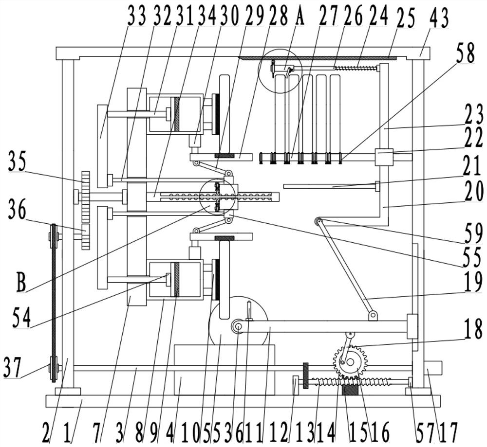
[0027] see Figure 1-6 , a cutting device for chip processing, comprising a base plate 1, and also comprising:

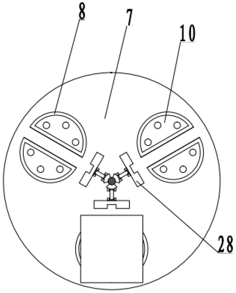
[0028] The enclosure plates 2 are fixedly arranged on both sides of the bottom plate 1, the top of the enclosure plate 2 is fixedly connected to the top plate 43, and one side of the enclosure plate 2 is rotatably connected to the feeding tray 7;

[0029]The cutting mechanism 53 arranged on one side of the feeding tray 7 includes an installation rod 11 , which is slidably connected to the side wall of the enclosure 2 , and one end of the installation rod 11 is rotatably connected to the cutting wheel 5 . The top end is fixedly connected to the push rod 6, the side wall of the feeding plate 7 is fixedly connected to the piston cylinder 8, the piston cylinder 8 is provided with a piston assembly 54, one end of the piston cylinder 8 is fixedly connected to the adsorption disk 10, and the adsorption disk 10 is provided with air holes, so The side wall of the piston cyl...

Embodiment 2

[0032] see Figure 1-6 , the other content of this embodiment is the same as that of Embodiment 1, the difference is that: the linkage assembly 55 includes a sliding block 39, the sliding block 39 is slidably connected with the bearing beam 34, and one end of the sliding block 39 is hinged to the linkage arm 29, and the linkage One end of the arm 29 is hingedly connected to the stopper plate 28, the bearing beam 34 on one side of the sliding block 39 is fixedly connected to the stopper protrusion 42, the side wall of the sliding block 39 is fixedly connected to the positioning block 38, and the positioning block 38 slides through A stop column 40 is provided, a telescopic piece 41 is sleeved on the stop column 40, and both ends of the telescopic piece 41 are respectively fixedly connected with the positioning block 38 and one end of the stop column 40. In actual use, the sliding block 39 moves and can pass the linkage arm 29. The stopper plate 28 is driven to move up and down,...


PUM


Abstract

The invention discloses a cutting device for chip processing, and relates to the technical field of chip cutting, the cutting device comprises a bottom plate and further comprises surrounding plates fixedly arranged on the two sides of the bottom plate, the tops of the surrounding plates are fixedly connected with a top plate, and one side of each surrounding plate is rotationally connected with a feeding disc; the cutting mechanism is arranged on one side of the feeding disc and comprises a mounting rod, the mounting rod is in sliding connection with the side wall of the surrounding plate, one end of the mounting rod is rotationally connected with a cutting wheel, a linkage assembly drives a piston assembly to move, negative pressure is generated in a piston cylinder, meanwhile, a stop plate is driven to move, and rapid fixing and limiting of chips are achieved; meanwhile, the mounting rod moves up and down to drive the cutting wheel to move up and down, high-quality continuous cutting is achieved, and then the cut chips are rapidly recycled; and a supporting piece is fixedly connected between the stop block and the pushing arm, a movable assembly is arranged at the bottom of the movable block, meanwhile, the movable assembly makes contact with the linkage assembly, the piston assembly is triggered, and automatic feeding and positioning of chips are achieved.

Description

technical field [0001] The invention relates to the technical field of chip cutting, in particular to a cutting device for chip processing. Background technique [0002] In the semiconductor manufacturing process, a semiconductor chip including a semiconductor active device and an interconnect structure arranged on the device can be formed on a semiconductor substrate through advanced manufacturing processes such as photolithography, etching and deposition, and multiple semiconductor chips can be formed on one wafer. Finally, these chips are cut from the wafer, and the packaging process is carried out to form integrated circuit devices. [0003] The traditional chip processing and cutting device generally places the workpiece manually, clamps it with a positioning device, then cuts it, and finally takes it manually. Although this operation process realizes the cutting and processing of the chip, the manual operation steps in the whole process are relatively In the current e...

Claims


Application Information

Patent Timeline
Patent Type & Authority Applications(China)
IPC IPC(8): B28D5/02B28D7/00B28D7/04H01L21/78H01L21/677H01L21/683
CPCB28D5/023B28D5/0058B28D5/0082B28D5/0094H01L21/78H01L21/677H01L21/6838Y02P70/10
Inventor 陈莹谢烽
Owner 深圳市伟烽恒科技有限公司
Why Eureka
Try Eureka