
Multi-contact high-current high-voltage test probe

A technology for testing probes and high current, which is applied to the parts of electrical measuring instruments, measuring electronics, measuring devices, etc. It can solve the problems of burning out test equipment, easy to burn out, and discarding probes, so as to reduce the measurement time , the effect of reducing damage

Pending Publication Date: 2022-07-29
苏州伊欧陆系统集成有限公司
View PDF5 Cites 0 Cited by
  • Summary
  • Abstract
  • Description
  • Claims
  • Application Information

AI Technical Summary

Problems solved by technology

[0004] 1. When the test current is too large, it will cause the high current to burn out the test equipment and fail to achieve the test effect
[0005] 2. When the tested chip is a high-current chip, the power is relatively large, and the ability to conduct a large current cannot be achieved.
[0006] 3. The tip of the probe is mostly exposed, and the probe is easily damaged. In the high-temperature test environment, it is easy to burn out. After the probe is used to the maximum, the tip of the probe will be worn out, and the probe is forced to be discarded.

Method used


Image

  • Multi-contact high-current high-voltage test probe
  • Multi-contact high-current high-voltage test probe
  • Multi-contact high-current high-voltage test probe

Examples


Embodiment Construction

[0027] In order to make the above objects, features and advantages of the present invention more clearly understood, the specific embodiments of the present invention will be described in detail below with reference to the accompanying drawings. In the following description, numerous specific details are set forth in order to provide a thorough understanding of the present invention. However, the present invention can be implemented in many other ways different from those described herein, and those skilled in the art can make similar improvements without departing from the connotation of the present invention. Therefore, the present invention is not limited by the specific embodiments disclosed below.

[0028] Unless otherwise defined, all technical and scientific terms used herein have the same meaning as commonly understood by one of ordinary skill in the art to which this invention belongs. The terms used herein in the description of the present invention are for the purpo...


PUM

PropertyMeasurementUnit
lengthaaaaaaaaaa
widthaaaaaaaaaa
thicknessaaaaaaaaaa

Abstract

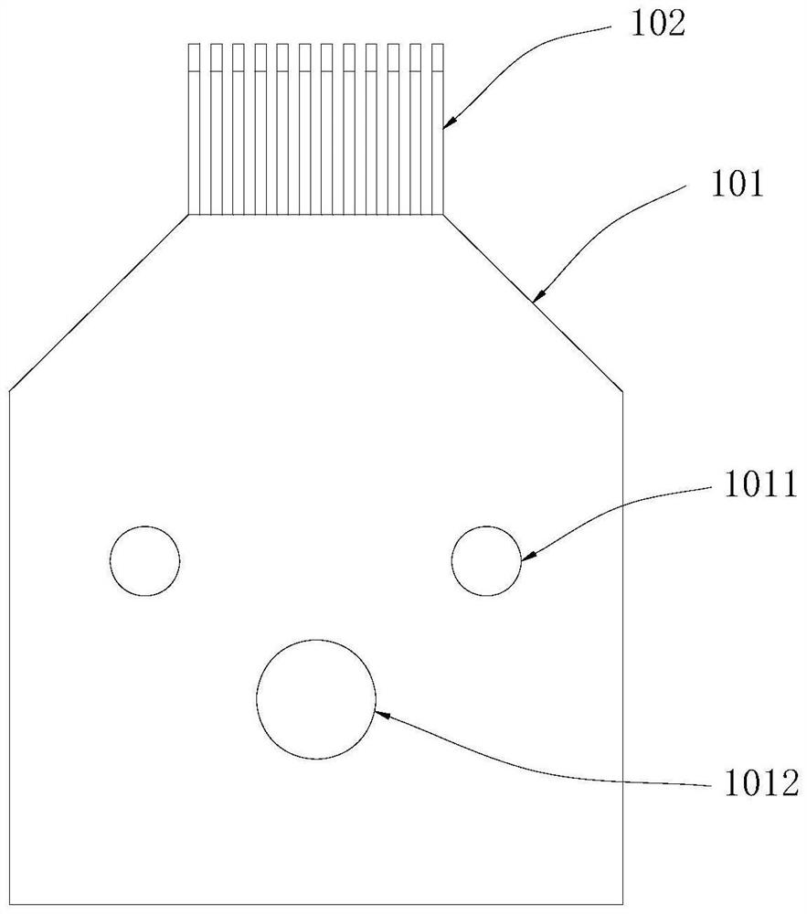
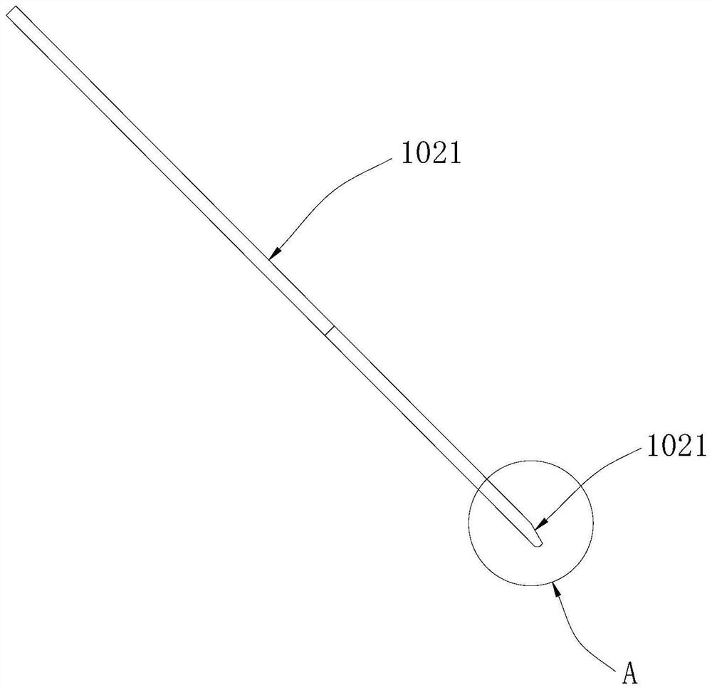
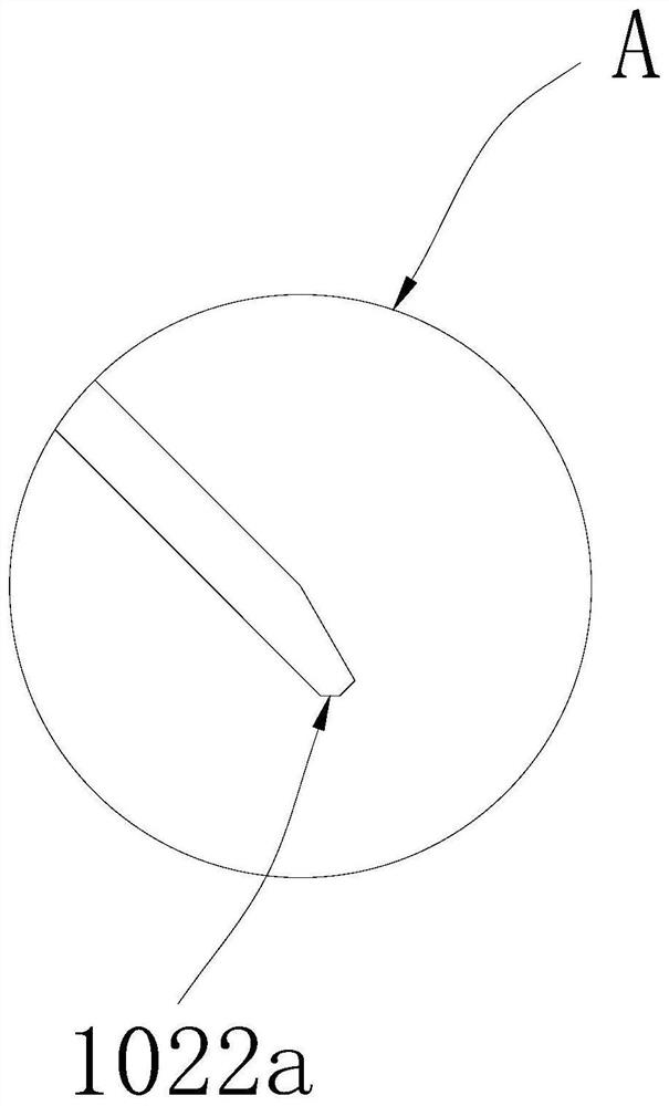
The invention discloses a multi-contact high-current high-voltage test probe which comprises a probe plate, a plurality of pins are arranged at the front end of the probe plate, and a plurality of limiting holes and mounting holes are formed in the middle of the probe plate; the surface of the multi-contact high-current high-voltage test probe is integrally plated with gold. A multi-pin design is adopted, a multi-point contact technology is realized, so that uniform current distribution is realized, the contact resistance of a pin test area and a test bonding pad is extremely small, the measurement work of 10kV high voltage and 300A pulse high current under a coaxial condition can be realized through single contact, a plurality of probes are not needed, and the cost is reduced. And the high-current and high-voltage test work is simpler and more convenient. And the damage to the test probe and the test bonding pad can be reduced to the greatest extent.

Description

technical field [0001] The invention relates to the technical field of integrated circuit testing, in particular to a multi-contact high-current and high-voltage testing probe. Background technique [0002] The measurement of the quality of semiconductor device testing of semiconductor chips or wafers, a probe that transmits a test signal (current or voltage) to the semiconductor device, and it is very important to transmit the test signal stably, the probe has a A predetermined test signal is applied to the probes of the semiconductor device pads. [0003] The quality of the general test probe is mainly reflected in the material, coating, and production process, and there are the following shortcomings: [0004] 1. When the test current is too large, it will cause the high current to burn out the test equipment and fail to achieve the test effect. [0005] 2. When the tested chip is a high-current chip, the power is large, and the ability to conduct high current cannot be...

Claims


Application Information

Patent Timeline
Patent Type & Authority Applications(China)
IPC IPC(8): G01R1/073
CPCG01R1/07314Y02E10/50
Inventor 刘权张海洋刘伟吕文波
Owner 苏州伊欧陆系统集成有限公司
Learn More