

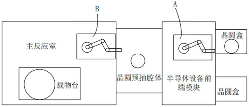
Wafer conveying device, wafer pre-pumping device and rapid wafer conveying system
A transfer device and wafer technology, applied to conveyor objects, transportation and packaging, electrical components, etc., can solve the problems of low efficiency, long transfer time, and low production capacity, so as to reduce the transfer time and improve Stability, speed-up effects
- Summary
- Abstract
- Description
- Claims
- Application Information
AI Technical Summary
Problems solved by technology
Method used
Image

Examples
Embodiment Construction
[0072] In order to make the above and other features and advantages of the present invention more apparent, the present invention is further described below with reference to the accompanying drawings. It should be understood that the specific embodiments given herein are for the purpose of explaining to those skilled in the art, and are merely illustrative and not restrictive.
[0073] In the description of the present invention, it should be understood that the terms "center", "longitudinal", "lateral", "length", "width", "thickness", "upper", "lower", "front", " Rear, Left, Right, Vertical, Horizontal, Top, Bottom, Inner, Outer, Clockwise, Counterclockwise, Axial, The orientations or positional relationships indicated by "radial direction", "circumferential direction", etc. are based on the orientations or positional relationships shown in the accompanying drawings, which are only for the convenience of describing the present invention and simplifying the description, rathe...
PUM
 Abstract
Description
Claims
Application Information