Wafer alignment device and alignment method

A technology for aligning devices and wafers, applied in semiconductor/solid-state device testing/measurement, electrical components, circuits, etc., can solve problems such as complex structure and difficult debugging, and achieve compact structure, precise movement and power-off retention Effect

Pending Publication Date: 2022-07-29
BEIJING U PRECISION TECH
View PDF0 Cites 4 Cited by
  • Summary
  • Abstract
  • Description
  • Claims
  • Application Information

AI Technical Summary

Problems solved by technology

The position of the air bearing base can be measured by the grating ruler in the X and Y direction moving components. Theoretically, the position of the objective lens at the end of the C-arm is also known. When the air bearing base remains stationary, the C-arm is theoretically stationary and the vision The system also keeps still during image acquisition, so the measured position difference between the upper and lower wafer marks is the position difference between the upper and lower wafers, but due to the complex structure, it is relatively difficult to debug

Method used


Image

  • Wafer alignment device and alignment method
  • Wafer alignment device and alignment method
  • Wafer alignment device and alignment method

Examples


Embodiment Construction

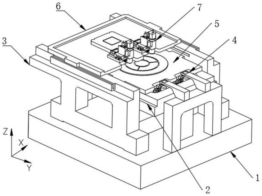
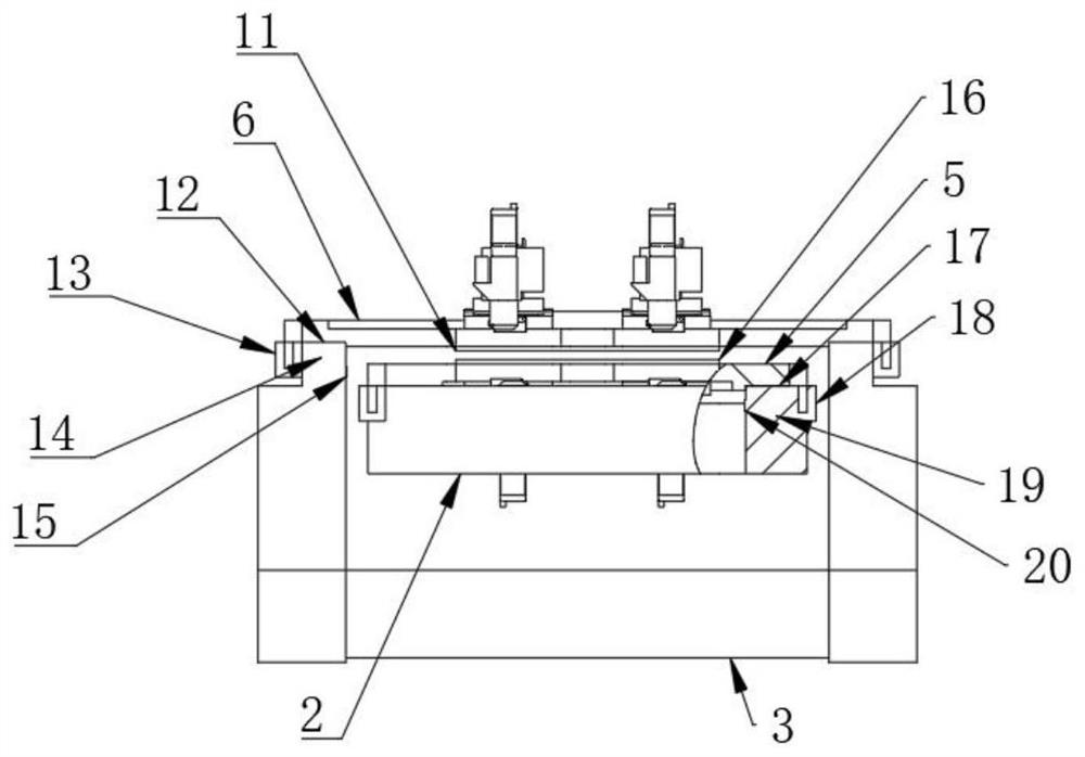
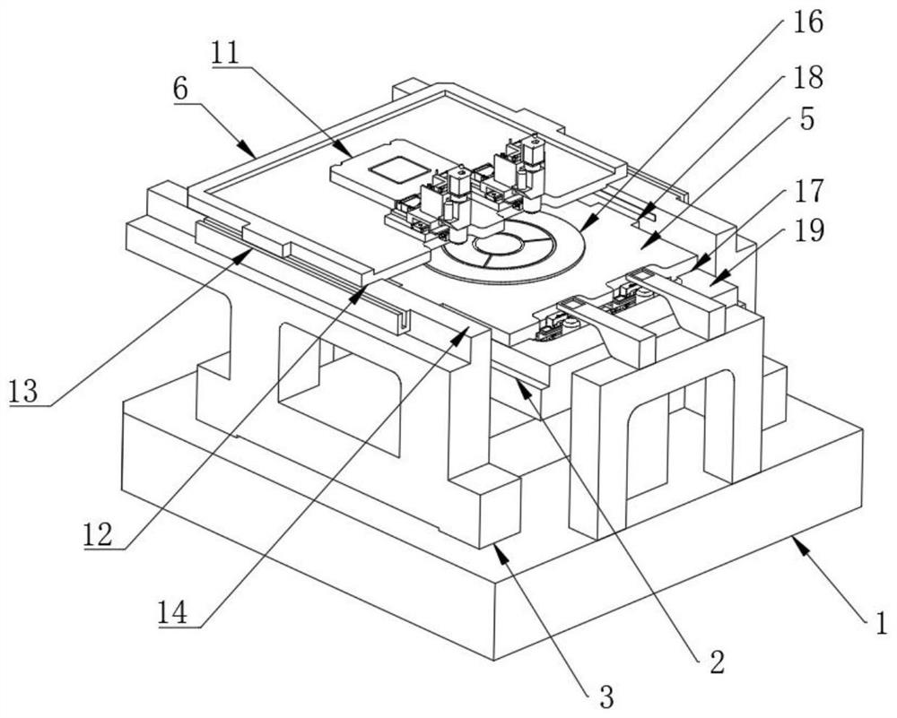
[0044] like Figure 1-3 As shown, a wafer alignment device includes a base 1, a lower motion stage 2 and an upper motion stage 3 are arranged above the base 1, two alignment marks 4 are installed on the base 1, and the upper The motion platform 3 is provided with an upper bearing platform 6 , and the lower motion platform 2 is provided with a lower bearing platform 5 ; two sets of vision systems 7 are respectively provided above the upper bearing platform 6 and below the lower bearing platform 5 .

[0045] Each set of vision systems 7 can move independently in X and Z directions. The two sets of vision systems above the upper platform 6 may be referred to as upper vision systems, and the two sets of vision systems below the lower platform 5 may be referred to as lower vision systems.

[0046] The base is made of marble, the upper surface of which is an air-floating surface, and the bottom of the upper motion table 3 is an air-floating block, which can float and fall on the su...


PUM


Abstract

The invention relates to the technical field of semiconductor processing, in particular to a wafer alignment device and an alignment method. The device comprises a base, a lower movement table and an upper movement table are arranged above the base, calibration marks are arranged on the base, an upper bearing table is arranged on the upper movement table, and a lower bearing table is arranged on the lower movement table; and two sets of visual systems are respectively arranged above the upper bearing platform and below the lower bearing platform. According to the wafer alignment device, a C-shaped arm visual system is omitted, the independent visual system is used for achieving the measurement function, the visual system is not provided with a cantilever structure, and the movement amount of a microscopic part can be directly measured. Before the upper wafer and the lower wafer are finally attached, the relative position change of the upper wafer and the lower wafer can be measured all the time for final compensation.

Description

technical field [0001] The present invention relates to the technical field of semiconductor processing, in particular to a wafer alignment device and an alignment method. Background technique [0002] With the development of science and technology, image processing hardware technology has made rapid progress, and the application of image recognition technology has become more and more extensive. By collecting the data information and analyzing it to obtain key information, so as to meet the development needs of various industries. In the semiconductor industry, image recognition and processing techniques are often combined with microscopic imaging to inspect the quality of microscopic patterns on wafer surfaces, or to measure wafer position. [0003] Bonding is a process in which multiple chips are stacked together, and vertical vias are used to achieve electrical connection between the chips. It has been widely regarded as a way to go beyond "Moore's Law". 3D interconnec...

Claims


Application Information

Patent Timeline
Patent Type & Authority Applications(China)
IPC IPC(8): H01L21/68H01L21/66
CPCH01L21/681H01L22/12H01L22/20
Inventor 张昊司伟田陈陈谭永旭
Owner BEIJING U PRECISION TECH
Why Eureka
Try Eureka